Method and system for configuring chip connection mode

A connection method and chip configuration technology, which is applied in the direction of electrical connection of printed components, printed circuits connected with non-printed electrical components, special data processing applications, etc., can solve problems such as single-layer wiring connections

Pending Publication Date: 2019-12-31
BEIJING BITMAIN TECH LTD
View PDF6 Cites 0 Cited by
  • Summary
  • Abstract
  • Description
  • Claims
  • Application Information

AI Technical Summary

Problems solved by technology

[0006] The present invention provides a method and system for configuring chip connection methods to solve the problem of how to connect multiple chips on a PCB board with single-layer wiring

Method used


Image

  • Method and system for configuring chip connection mode
  • Method and system for configuring chip connection mode
  • Method and system for configuring chip connection mode

Examples


Embodiment Construction

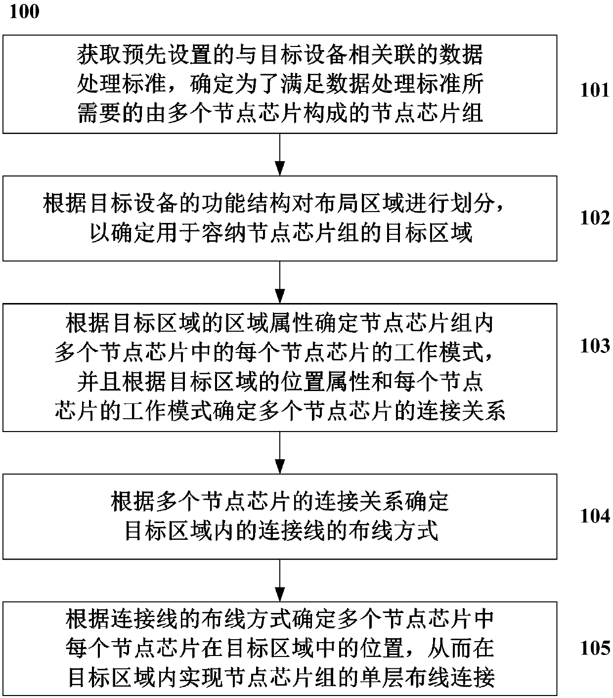
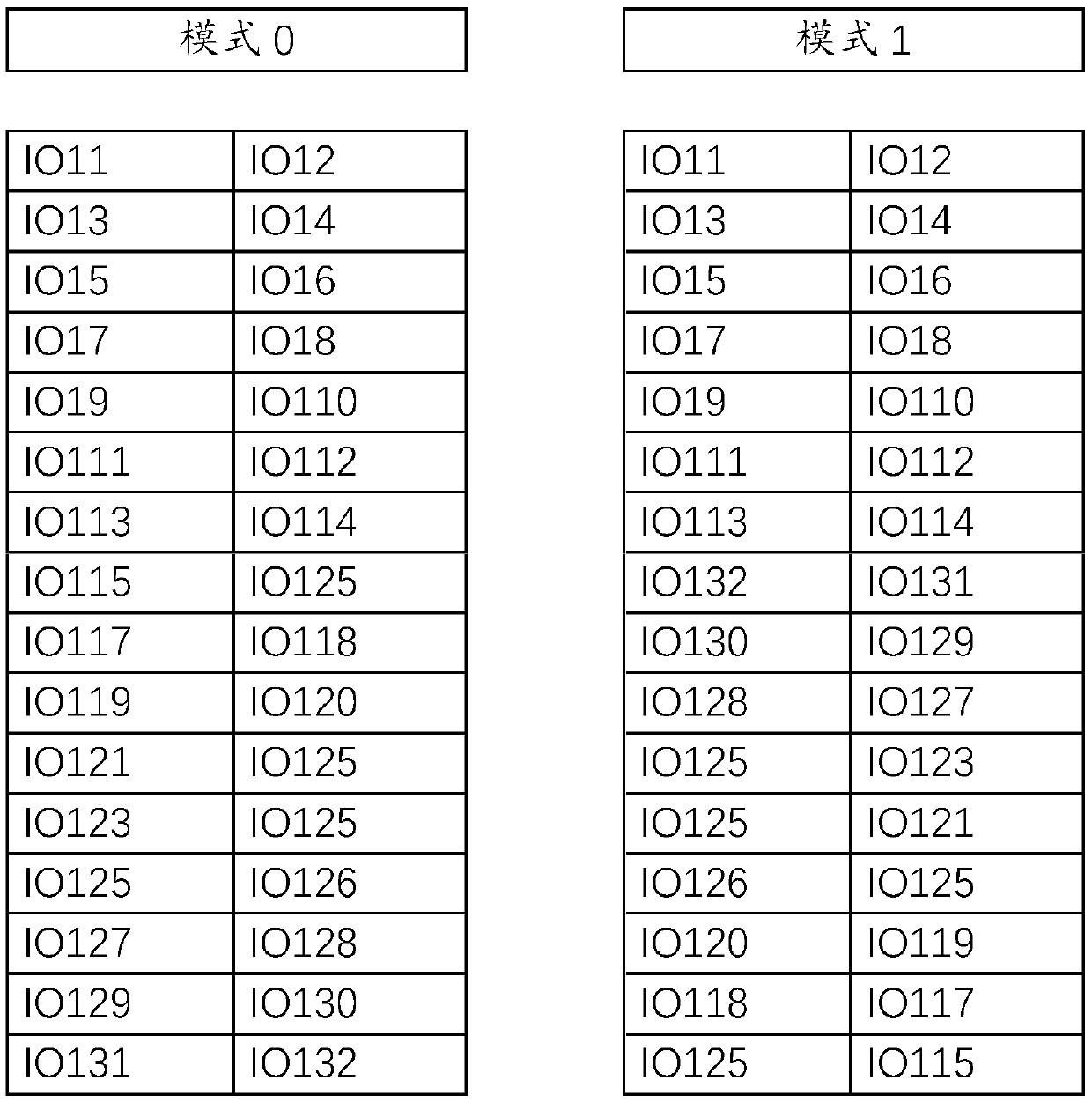
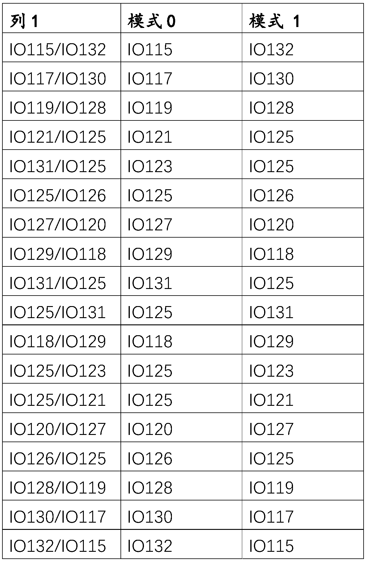
[0055] Exemplary embodiments of the present invention will now be described with reference to the drawings; however, the present invention may be embodied in many different forms and are not limited to the embodiments described herein, which are provided for the purpose of exhaustively and completely disclosing the present invention. invention and fully convey the scope of the invention to those skilled in the art. The terms used in the exemplary embodiments shown in the drawings do not limit the present invention. In the figures, the same units / elements are given the same reference numerals.

[0056] Unless otherwise specified, the terms (including scientific and technical terms) used herein have the commonly understood meanings to those skilled in the art. In addition, it can be understood that terms defined by commonly used dictionaries should be understood to have consistent meanings in the context of their related fields, and should not be understood as idealized or over...


PUM


Abstract

The invention discloses a method for configuring a chip connection mode. The method includes: acquiring a data processing standard associated with the target device, and determining a node chipset composed of a plurality of node chips and required to meet the data processing standard, each node chip in the plurality of node chips being capable of working according to any one of a plurality of working modes; dividing the layout area according to the functional structure of the target equipment, and determining a target area for accommodating the node chipset; determining the working mode of each node chip in the plurality of node chips in the node chip group according to the region attribute of the target region, and determining the connection relationship of the plurality of node chips according to the position attribute of the target region and the working mode of each node chip; determining a wiring mode of a connecting line in the target area according to the connection relationshipof the plurality of node chips; and determining the position of each node chip in the target area according to the wiring mode to realize single-layer wiring connection of the node chip group.

Description

technical field [0001] The present invention relates to the technical field of chip connection, and more particularly, to a method and system for configuring a chip connection mode. Background technique [0002] The Chinese name of PCB (Printed Circuit Board) is printed circuit board, also known as printed circuit board, which is an important electronic component, a support for electronic components, and a carrier for electrical connection of electronic components. In order to realize its circuit function, the PCB board usually needs to perform wiring operations on the PCB board, that is, to arrange the wiring connection between components on the PCB board, first lay the wires, and pass the wires through the holes where the pins with electrical connections are located. , so that the connection between components can be realized while soldering the components, and then the circuit function of the PCB board can be realized. [0003] In the field of large amount of computation...

Claims


Application Information

Patent Timeline
IPC IPC(8): G06F17/50
CPCH05K1/11H05K1/18Y02D10/00
Inventor 杨存永杨英
Owner BEIJING BITMAIN TECH LTD
Why Eureka
Try Eureka