An output drive circuit against ground bounce noise

A technology for outputting drive circuits and ground bounce noise, which is applied in the field of semiconductor integrated circuits, can solve problems such as large current change rate, ground bounce noise, and large power consumption, so as to reduce dynamic current, improve ground bounce noise resistance, and improve The effect of driving ability

Active Publication Date: 2021-01-08
BEIJING MXTRONICS CORP +1
View PDF20 Cites 0 Cited by
  • Summary
  • Abstract
  • Description
  • Claims
  • Application Information

AI Technical Summary

Problems solved by technology

[0005] like figure 2 As shown, in the traditional three-state output driving circuit, when the output level changes, the PMOS output transistor PM and the NMOS output transistor NM will be turned on at the same time within a certain period of time, which not only causes a large current change rate, but also leads to a large Ground bounce noise, but also a large power consumption

Method used


Image

  • An output drive circuit against ground bounce noise
  • An output drive circuit against ground bounce noise
  • An output drive circuit against ground bounce noise

Examples


Embodiment

[0054] The working principle will be described below in conjunction with the input waveforms at the gate terminals for outputting and driving the PMOS transistor and the NMOS transistor in a specific embodiment of the present invention.

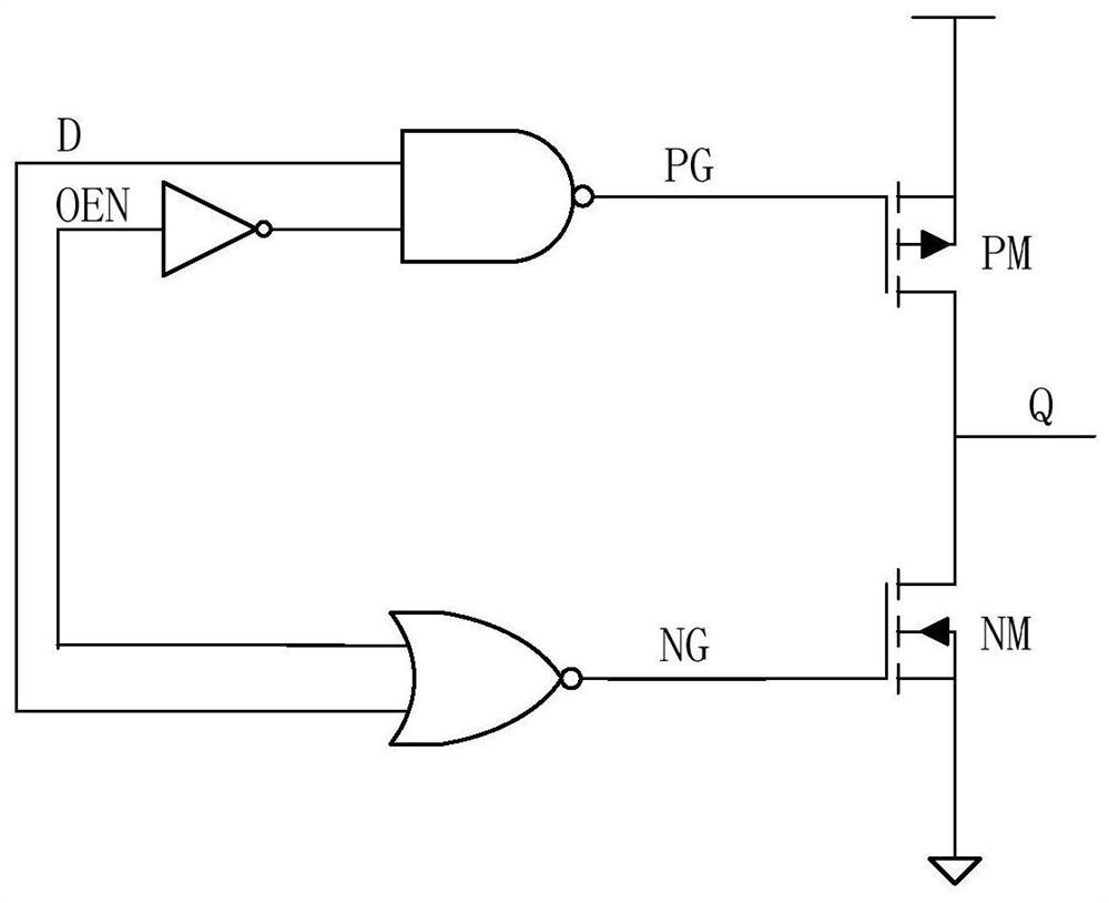
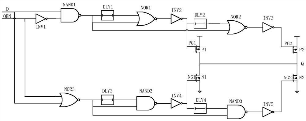
[0055] use image 3 The circuit structure in produces as Figure 6 The shown gate drive signals PG1 and NG1 ensure that the PMOS transistor and the NMOS transistor are not turned on at the same time.

[0056] In order to reduce the ground bounce noise, the output driving PMOS transistor is divided into two parts, the first PMOS transistor P1 and the second PMOS transistor P2, and the output driving NMOS transistor is divided into two parts, the first NMOS transistor N1 and the second NMOS transistor N2, wherein The width-to-length ratio of the first PMOS transistor P1 is smaller than that of the second PMOS transistor P2, and the width-to-length ratio of the first NMOS transistor N1 is smaller than that of the second NMOS transistor N2. Whe...


PUM


Abstract

The invention relates to an output driving circuit capable of resisting ground bounce noise, and belongs to the field of semiconductor integrated circuits. According to the output driving circuit, certain time delay is introduced in the switching conversion process of an output driving PMOS transistor and an NMOS transistor by adding a logic circuit to avoid simultaneous conduction of the PMOS transistor and the NMOS transistor, and different driving capacities of the circuit in the static state and in the switching process are realized by making the driving transistors with different width-to-length ratios switched on successively. The output driving circuit can reduce the ground bounce noise, and has high driving capacity.

Description

technical field [0001] The invention relates to an output drive circuit against ground bounce noise, which belongs to the field of semiconductor integrated circuits. Background technique [0002] As the integration level of CMOS integrated circuits is getting higher and higher, the operating frequency is getting faster and faster, and there are more and more input and output pins, the synchronous switching noise is correspondingly larger. Synchronous switching noise will not only cause the jitter of the power supply and ground plane of the chip, but also affect the delay and distortion of other output signals. What is more serious is that if its maximum amplitude exceeds the threshold voltage of the transistor, the circuit will not work properly. . The output unit is the main noise source of synchronous switching noise, because the switching current flowing through the ground pin of the chip changes very rapidly, and the parasitic inductance of the package is also relativel...

Claims


Application Information

Patent Timeline
Patent Type & Authority Patents(China)
IPC IPC(8): H02M1/088H02M1/32
CPCH02M1/088H02M1/32
Inventor 李健胡贵才孔瀛樊旭穆辛
Owner BEIJING MXTRONICS CORP
Why Eureka
Try Eureka