

Display device and method for detecting state thereof
A display device and state detection technology, applied in static indicators, nonlinear optics, instruments, etc., can solve the problem that the driving circuit cannot easily detect abnormalities
- Summary
- Abstract
- Description
- Claims
- Application Information
AI Technical Summary
Problems solved by technology
Method used
Image


Examples
no. 1 approach
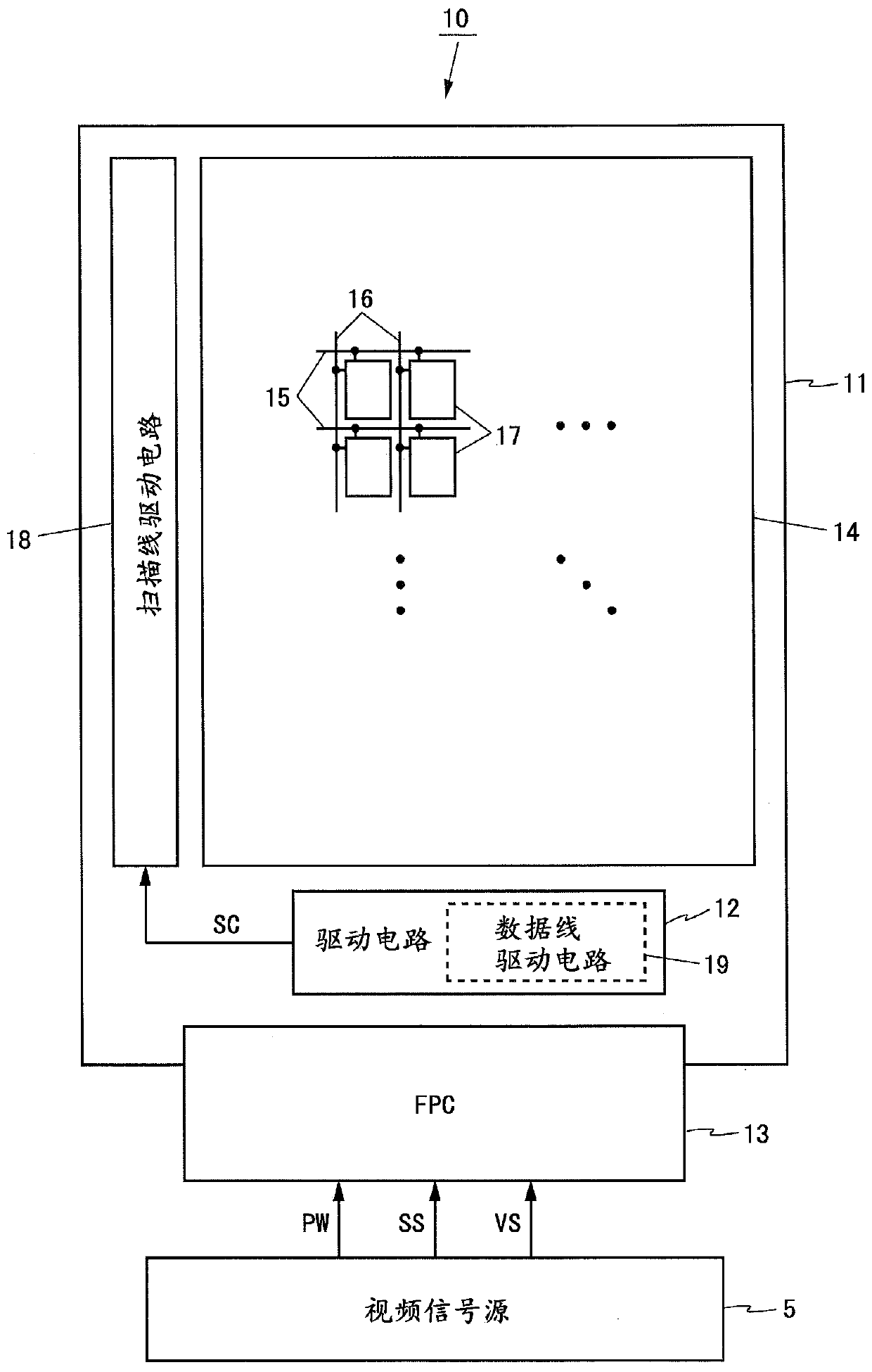
[0063] figure 1 It is a block diagram showing the configuration of the liquid crystal display device according to the first embodiment of the present invention. figure 1 The illustrated liquid crystal display device 10 has a liquid crystal panel 11 , a drive circuit 12 , and an FPC 13 . The drive circuit 12 is mounted on the liquid crystal panel 11 . The liquid crystal display device 10 is connected to the video signal source 5 during normal operation. Liquid crystal panel 11 and video signal source 5 are electrically connected using FPC13. The video signal source 5 supplies the liquid crystal panel 11 with a power supply voltage PW, a synchronization signal SS, and a video signal VS through the FPC 13 . FPC 13 functions as a connection portion that electrically connects liquid crystal panel 11 and video signal source 5 .
[0064] The liquid crystal panel 11 includes a display unit 14 . The display unit 14 includes a plurality of scan lines 15 , a plurality of data lines ...
no. 2 approach
[0092] Image 6 It is a diagram showing a connection state when testing the liquid crystal display device according to the second embodiment. Image 6 The illustrated liquid crystal display device 70 has a liquid crystal panel 71 , a drive circuit 12 and an FPC 73 . Among the constituent elements of the present embodiment, the same elements as those of the first embodiment are denoted by the same reference numerals, and description thereof will be omitted. Differences from the first embodiment will be described below.
[0093] In liquid crystal display device 70 , drive circuit 12 is mounted not on liquid crystal panel 11 but on FPC 13 . The bumps 57 of the drive circuit 12 are connected to the data lines 16 via wiring (not shown) formed on the FPC and wiring (not shown) formed on the liquid crystal panel 11 . The bumps 58 of the driving circuit 12 are electrically connected to the scanning line driving circuit 18 through the wiring formed on the FPC and the wiring formed o...
PUM
 Abstract
Description
Claims
Application Information