
Array substrate and manufacturing method thereof

A technology of an array substrate and a manufacturing method, which is applied in the field of substrates and their manufacturing, can solve problems such as reducing the overall screen ratio, and achieve the effect of reducing usage

Active Publication Date: 2020-01-17
WUHAN CHINA STAR OPTOELECTRONICS SEMICON DISPLAY TECH CO LTD
View PDF6 Cites 2 Cited by
  • Summary
  • Abstract
  • Description
  • Claims
  • Application Information

AI Technical Summary

Problems solved by technology

[0006] In view of this, the present invention provides an array substrate and a manufacturing method thereof, so as to solve the problem in the prior art that the boundary formed by the parallel arrangement of the winding area and the plurality of groove structures reduces the screen ratio of the full screen. question

Method used


Image

  • Array substrate and manufacturing method thereof
  • Array substrate and manufacturing method thereof
  • Array substrate and manufacturing method thereof

Examples


Embodiment Construction

[0025] The following descriptions of the various embodiments refer to the accompanying drawings to illustrate specific embodiments in which the present invention can be practiced. Furthermore, the directional terms mentioned in the present invention are, for example, up, down, top, bottom, front, back, left, right, inside, outside, side, surrounding, central, horizontal, transverse, vertical, longitudinal, axial, The radial direction, the uppermost layer or the lowermost layer, etc. are only directions referring to the attached drawings. Therefore, the directional terms used are used to illustrate and understand the present invention, but not to limit the present invention.

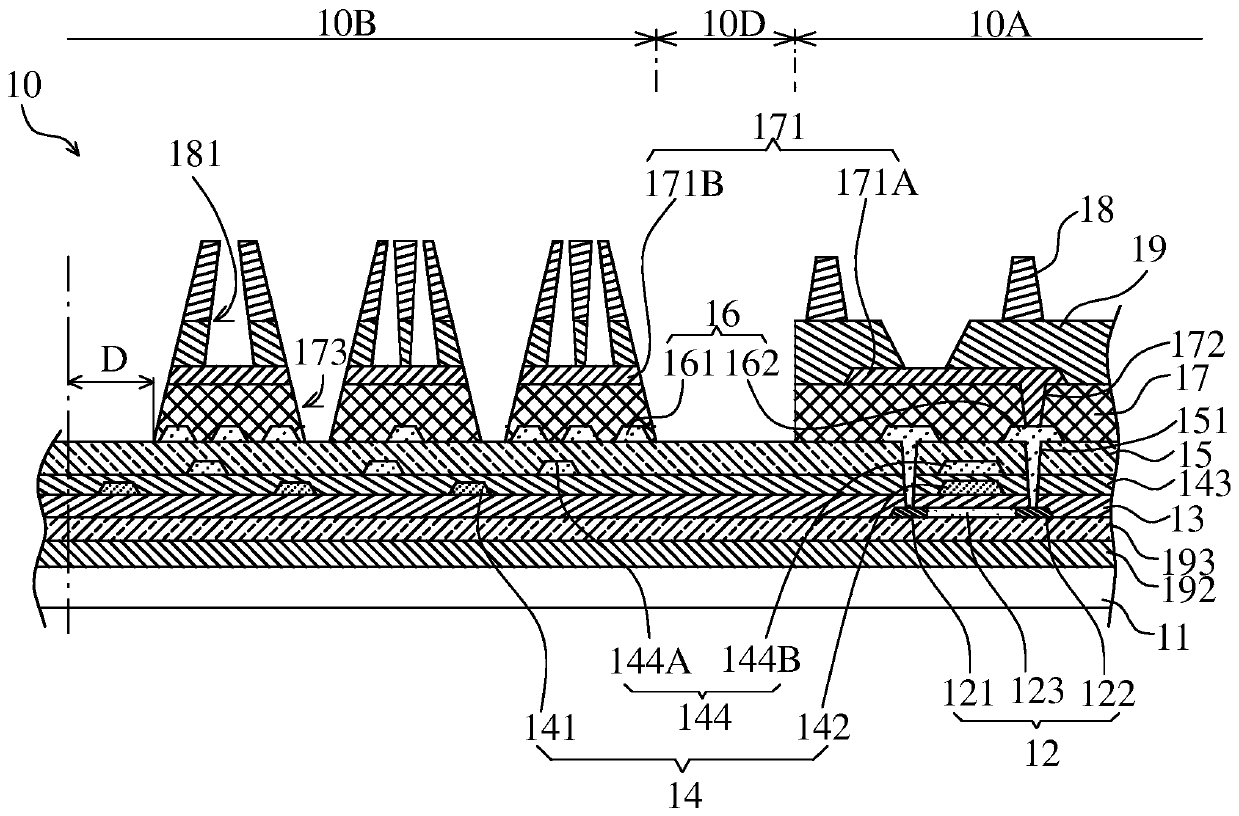
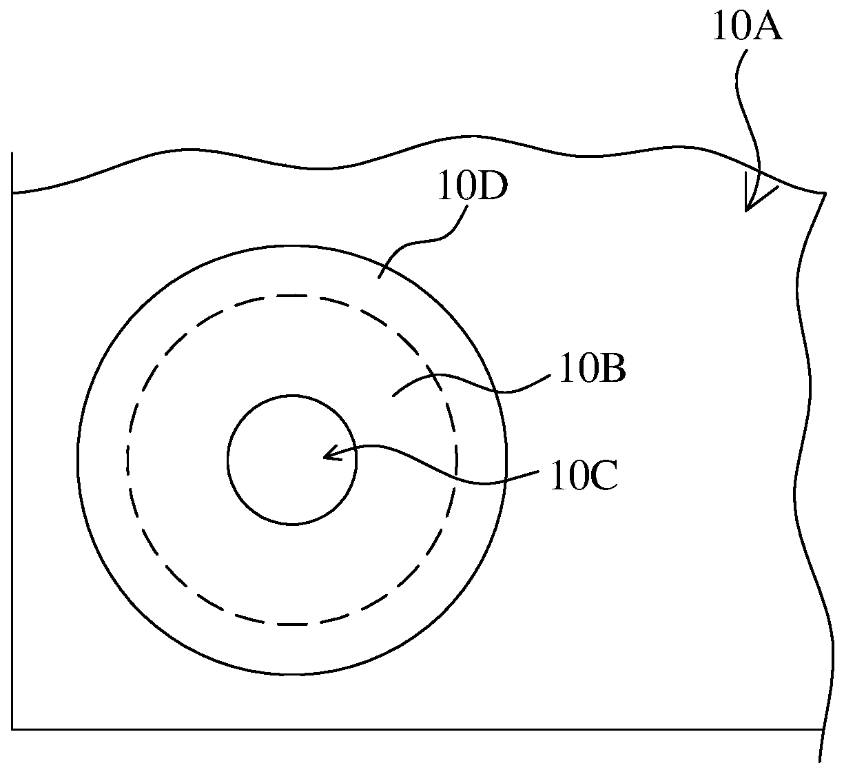
[0026] Please refer to Figure 1A and 1B , the array substrate 10 according to an embodiment of the present invention includes a display area (active area; AA) 10A and a wiring area 10B. In one embodiment, the array substrate 10 further includes an opening area 10C, wherein the wiring area 10B is locate...


PUM


Abstract

The invention discloses an array substrate and a manufacturing method thereof. The array substrate comprises a display area and a winding area, wherein the array substrate comprises a substrate, an active layer, a first insulating layer, a first metal layer, a second insulating layer, a second metal layer, a third insulating layer, a third metal layer, a patterned flat layer, a pixel defining layer and a supporting layer. The first metal layer comprises at least one first wiring pattern arranged on the first insulating layer in the winding area, the second metal layer comprises at least one second wiring pattern arranged on the second insulating layer in the winding area, the third metal layer comprises at least one third wiring pattern arranged on the third insulating layer in the windingarea, and the pixel defining layer and the supporting layer in the winding area jointly have at least one undercut structure. According to the array substrate and the manufacturing method thereof, the width of a boundary formed by the winding area can be reduced.

Description

technical field [0001] The present invention relates to a substrate and a manufacturing method thereof, in particular to an array substrate and a manufacturing method thereof. Background technique [0002] Full screen is one of the goals of OLED display technology development. The current under-display camera technology is mainly through forming a hole in the display panel for accommodating a camera. However, the above-mentioned hole is formed by removing the base substrate of a camera area, so it is easy to affect the packaging effect, and has the problem of poor reliability. [0003] In order to solve the above problems, the prior art is to provide a plurality of groove structures under the transistor structure of the array substrate at positions adjacent to the hole (for example, at the boundary between a display area and the camera area), Each of the plurality of groove structures has an undercut structure. During subsequent encapsulation steps, an organic layer (or i...

Claims


Application Information

Patent Timeline
Patent Type & Authority Applications(China)
IPC IPC(8): H01L27/32
CPCH10K59/00H10K59/124H10K59/12H10K59/1315H10K59/1201
Inventor 陈诚
Owner WUHAN CHINA STAR OPTOELECTRONICS SEMICON DISPLAY TECH CO LTD
Features
  • Generate Ideas
  • Intellectual Property
  • Life Sciences
  • Materials
  • Tech Scout
  • Unparalleled Data Quality
  • Higher Quality Content
  • 60% Fewer Hallucinations
Learn More