An exposure method for controlling batch line width differences of flexible circuit boards

A technology of flexible circuit board and exposure method, which is applied in the field of circuit boards, can solve the problems of narrowing line spacing and large line width, and achieve the effects of shortening the manufacturing cycle, reducing production costs, and simple operation

Active Publication Date: 2022-05-10
江苏上达半导体有限公司
View PDF4 Cites 0 Cited by
  • Summary
  • Abstract
  • Description
  • Claims
  • Application Information

AI Technical Summary

Problems solved by technology

[0011] The purpose of the present invention is to provide an exposure method for controlling the difference in line width of flexible circuit board batches, so as to solve the problems of increasing line width and narrowing line spacing in the prior art

Method used


Image

  • An exposure method for controlling batch line width differences of flexible circuit boards
  • An exposure method for controlling batch line width differences of flexible circuit boards
  • An exposure method for controlling batch line width differences of flexible circuit boards

Examples


Embodiment Construction

[0026] The present invention will be described in further detail below in conjunction with the accompanying drawings and embodiments.

[0027] Firstly, the nouns in the present invention will be explained.

[0028] The products mentioned in this article refer to flexible circuit boards.

[0029] Photoresist—a photosensitive solder resist that reacts with light to produce a substance soluble in a specific chemical solution Coating—a method of attaching photoresist to a product through a device

[0030] Exposure - photosensitive treatment of the photoresist coated on the product to change the properties of the photoresist at the desired position

[0031] Development - removal of photoresists whose properties have changed after exposure

[0032] Line Width - the width of the wire

[0033] Line spacing - the distance between two adjacent conductors

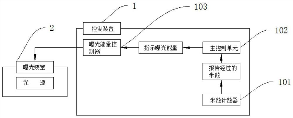
[0034] Such as figure 1 As shown, an exposure method for controlling the difference in line width of flexible circuit board ba...


PUM


Abstract

The invention discloses an exposure method for controlling the difference in line width of flexible circuit board batches. length value, the meter number counter feeds this signal back to the main controller; 3 the main controller generates a new signal after processing and transmits it to the exposure energy controller; 4 after the exposure energy controller receives the signal from the main controller, Control the amount of exposure light for the length of the next stage of the flexible circuit board; 5 repeat steps 1 to 4 until the exposure of all flexible circuit boards is completed. The invention weakens the diffusion of the photoresist by controlling the exposure energy, so as to control the deviation of the circuit due to the different time from exposure to development.

Description

technical field [0001] The invention relates to the technical field of circuit boards, in particular to an exposure method for controlling batch line width differences of flexible circuit boards. Background technique [0002] The production process of flexible circuit boards is: using the roll-to-roll production method, on a flexible circuit board substrate composed of a metal layer and an insulating film layer, a circuit pattern is formed by coating, exposure, development, etc., and then the circuit pattern is Electroplating, printing solder resist, etc. on the specific area of ​​the device, setting a protective layer, after that, electronic components such as ICs are mounted on the device holes, and finally, a single flexible circuit board is punched out from the flexible circuit board tape, and linked to other circuits board, used to produce electronic flexible circuit boards, the specific production steps are as follows: [0003] Step 1: Prepare a flexible circuit board...

Claims


Application Information

Patent Timeline
Patent Type & Authority Patents(China)
IPC IPC(8): G03F7/20
CPCG03F7/20G03F7/70491G03F7/70558
Inventor 叶新智杨洁孙彬沈洪李晓华
Owner 江苏上达半导体有限公司
Why Eureka
Try Eureka