Embedded touch display panel, driving method thereof and display device

A touch display panel, embedded technology, applied in the direction of instruments, electrical digital data processing, data processing input/output process, etc., can solve the problems of driving ability dependence, missed detection, increased power consumption and cost, etc.

Active Publication Date: 2020-02-04
KUSN INFOVISION OPTOELECTRONICS
View PDF4 Cites 0 Cited by
  • Summary
  • Abstract
  • Description
  • Claims
  • Application Information

AI Technical Summary

Problems solved by technology

However, the GDC lighting method is likely to cause missed detection of the integrated gate drive circuit (GIA, Gate In Array), and low grayscale defects (mura) cannot be tested. The display stage after the integrated circuit board is bound has too much driving capability for the integrated circuit board reliance, increasing power consumption and cost

Method used


Image

  • Embedded touch display panel, driving method thereof and display device
  • Embedded touch display panel, driving method thereof and display device
  • Embedded touch display panel, driving method thereof and display device

Examples


no. 1 example

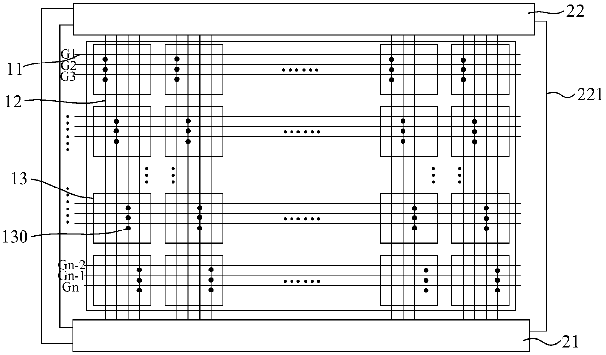
[0033] Please refer to figure 1 and figure 2 , figure 1 It shows a schematic structural diagram of an in-cell touch display panel according to the first embodiment of the present invention. The working phase of the in-cell touch display panel includes a detection phase and a display phase, and the detection phase occurs between the integrated circuit board and the main body of the display panel. Before bonding (bonding), it is used to test the integrity of components and leads on the display panel, figure 2 A schematic structural diagram of the in-cell touch display panel in the detection stage is shown.

[0034] Please refer to figure 1 , the in-cell touch display panel of this embodiment includes a plurality of scanning lines 11 (scanning lines 11 include G1, G2, G3, ..., Gn-2, Gn-1, Gn), a plurality of touch connection lines 12 , a plurality of common electrodes 13 arranged in an array, a lower switch circuit 21 and an upper switch circuit 22 , and a plurality of touc...

no. 2 example

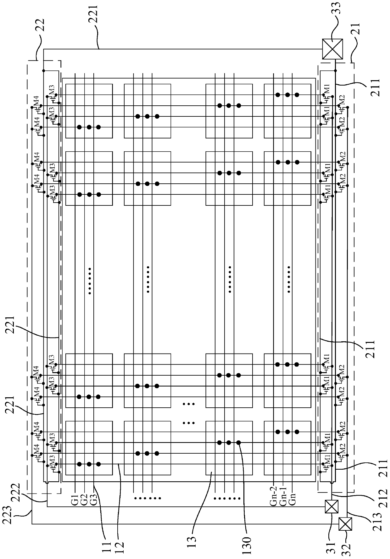
[0049] Please refer to Figure 5 and Figure 6 , Figure 5 It shows a schematic structural diagram of the in-cell touch display panel in the detection stage according to the second embodiment of the present invention, Figure 6 It is a structural schematic diagram of the embedded touch display panel in the display stage. The difference from the above-mentioned first embodiment is that the first gate switch line 211 and the second gate switch signal are not electrically connected through the third conductive pad 33 , and the in-cell touch display panel of this embodiment includes a fourth conductive pad 33 . The pad 34 , the fifth conductive pad 35 and the integrated circuit board 40 , the fourth conductive pad 34 is electrically connected to the first gate switch line 211 , and the fifth conductive pad 35 is electrically connected to the second gate switch line 221 .

[0050] The fourth conductive pad 34 receives the first gate switch signal input from the outside. The firs...

no. 3 example

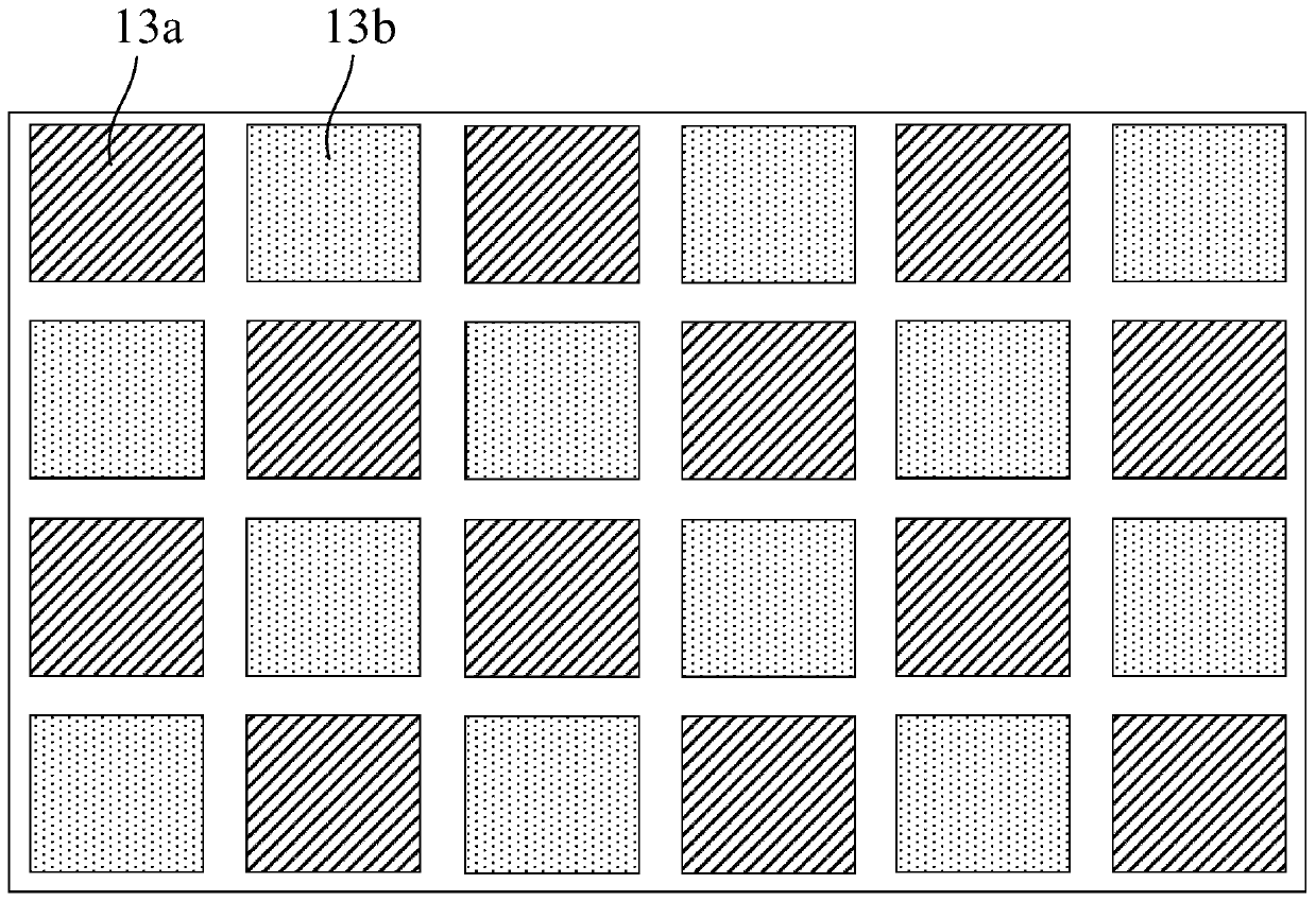
[0058] The third embodiment of the present invention provides an in-cell touch display panel, which is different from the second embodiment above in that the first common signal is inconsistent with the second common signal.

[0059] In the display stage, the second common signal is a compensation signal adjusted according to defects such as horizontal stripes, and the second common signal is used to superimpose and compensate the first common signal received by the common electrode 13 . Alternatively, the first common signal is a compensation signal adjusted according to defects such as stripes, and the first common signal is used to superimpose and compensate the second common signal received by the common electrode 13 .

[0060] Preferably, the in-cell touch display panel of this embodiment is a special-shaped display panel. Please refer to Figure 7 The special-shaped display panel includes a special-shaped area 51 and a non-special-shaped area 52, the upper switch circui...


PUM


Abstract

The invention discloses an embedded touch display panel, a driving method thereof and a display device, and belongs to the technical field of display. The embedded touch control display panel comprises a plurality of scanning lines, a plurality of touch control connecting lines and a plurality of common electrodes arranged in an array, the touch control connecting lines and the common electrodes are connected in a one-to-one correspondence mode, and the working stage of the embedded touch control display panel comprises a detection stage and a display stage. The embedded touch display panel further comprises a lower switching circuit and an upper switching circuit. The first end of each touch connecting line is connected with the lower switching circuit, and the second end of each touch connecting line is connected with the upper switching circuit; the lower switch circuit and the upper switch circuit input consistent test common signals to the two ends of the same touch control connecting line in the detection stage, each common electrode receives signals transmitted by the upper touch control connecting line and the lower touch control connecting line, the influence of scanning signal coupling on the signals on the touch control connecting lines is reduced, and transverse lines are prevented from appearing on a display image.

Description

technical field [0001] The present invention relates to the field of display technology, in particular to an in-cell touch display panel, a driving method thereof, and a display device. Background technique [0002] At present, in the field of display technology, touch display panels with touch functions have become more and more mainstream display products. Touch display panels are mainly divided into in-cell, on-cell and Plug-in. [0003] The existing in-cell touch display panel includes a plurality of common electrodes arranged in an array, the common electrodes are multiplexed as touch electrodes, and each common electrode is electrically connected to the integrated circuit board through a touch connection line. When the picture is displayed normally, since the signal output by the integrated circuit board will be delayed and attenuated when it is transmitted on the touch connection line, and the signals input to each common electrode are independent, the signal receive...

Claims


Application Information

Patent Timeline
Patent Type & Authority Applications(China)
IPC IPC(8): G06F3/041G06F3/044
CPCG06F3/0412G06F3/044
Inventor 赵中满陈尧魏齐严婷婷
Owner KUSN INFOVISION OPTOELECTRONICS
Why Eureka
Try Eureka