Transparent array substrate, transparent display panel, display panel and display terminal

A technology for transparent display panels and array substrates, applied in semiconductor devices, electrical components, circuits, etc., can solve problems such as affecting the overall consistency of the screen, unable to achieve full-screen display, etc., to increase the effective light-emitting area, improve clarity, improve The effect of the photosensitive effect

Active Publication Date: 2020-02-07
KUNSHAN GO VISIONOX OPTO ELECTRONICS CO LTD
View PDF5 Cites 18 Cited by
  • Summary
  • Abstract
  • Description
  • Claims
  • Application Information

AI Technical Summary

Problems solved by technology

[0002] With the rapid development of display terminals, users have higher and higher requirements for screen-to-body ratio. Since cameras, sensors, earpieces and other components need to be installed above the screen, a part of the area above the screen is usually reserved in the prior art for installing the above-mentioned Components, such as the front notch area of ​​the iPhone X, cannot achieve full-screen display, which affects the overall consistency of the screen

Method used


Image

  • Transparent array substrate, transparent display panel, display panel and display terminal
  • Transparent array substrate, transparent display panel, display panel and display terminal
  • Transparent array substrate, transparent display panel, display panel and display terminal

Examples


Embodiment Construction

[0076] In order to make the purpose, technical solutions and advantages of the embodiments of the present invention clearer, the technical solutions in the embodiments of the present invention will be clearly and completely described below in conjunction with the drawings in the embodiments of the present invention. Obviously, the described embodiments It is a part of embodiments of the present invention, but not all embodiments. Based on the embodiments of the present invention, all other embodiments obtained by those skilled in the art without creative efforts fall within the protection scope of the present invention.

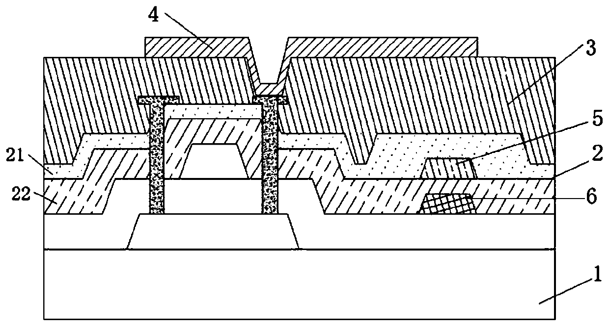
[0077] In describing the present invention, it should be understood that the terms "central", "lateral", "upper", "lower", "left", "right", "vertical", "horizontal", "top", " The orientation or positional relationship indicated by "bottom", "inner" and "outer" is based on the orientation or positional relationship shown in the drawings, and is only for the co...


PUM

PropertyMeasurementUnit
thicknessaaaaaaaaaa
wavelengthaaaaaaaaaa
transmittivityaaaaaaaaaa

Abstract

The invention discloses a transparent array substrate, a transparent display panel, a display panel and a display terminal. The transparent array substrate comprises a substrate, a pixel circuit, a first electrode, scanning lines and data lines, wherein the pixel circuit is arranged on the substrate, the first electrode is arranged on the pixel circuit and comprises a plurality of first electrodes, the scanning lines and the data lines are connected with the pixel circuit, the data lines and / or the scanning lines are arranged below the first pixel layer, the projection of the data lines on thesubstrate is first projection, the projection of the scanning lines is second projection, the projection of the plurality of first electrodes on the substrate is third projection, the first projection and the third projection are partially coincided and / or the second projection and the third projection are partially coincided, and the first electrodes, the scanning lines and the data lines are all transparent conductive materials. The data lines, the scanning lines and the first electrodes are arranged at different layers, the projection are arranged at edges of the first electrodes, thus, diffraction is reduced, meanwhile, the effective light-emitting areas of the first electrodes are expanded, and the aperture can be improved.

Description

technical field [0001] The present invention relates to the field of display technology, in particular to a transparent array substrate, a transparent display panel, a display panel and a display terminal. Background technique [0002] With the rapid development of display terminals, users have higher and higher requirements for screen-to-body ratio. Since cameras, sensors, earpieces and other components need to be installed above the screen, a part of the area above the screen is usually reserved in the prior art for installing the above-mentioned Components, such as the front notch area of ​​the iPhone X, cannot achieve full-screen display, which affects the overall consistency of the screen. Contents of the invention [0003] Based on this, it is necessary to provide a transparent array substrate, a transparent display panel, a display panel and a display terminal in order to solve the above technical problems. [0004] According to the first aspect, an embodiment of t...

Claims


Application Information

Patent Timeline
Patent Type & Authority Applications(China)
IPC IPC(8): H01L27/32
CPCH10K59/122H10K59/12H10K59/121H10K59/131
Inventor 许立雄张露
Owner KUNSHAN GO VISIONOX OPTO ELECTRONICS CO LTD
Why Eureka
Try Eureka