Unlock instant, AI-driven research and patent intelligence for your innovation.
Method for improving morphology of capacitor holes
What is Al technical title?
Al technical title is built by PatSnap Al team. It summarizes the technical point description of the patent document.
A technology of capacitance and morphology, which is applied in the direction of capacitors, circuits, electrical components, etc., can solve problems affecting the performance of memory, and achieve the effect of reducing the difficulty of lithography and etching
Active Publication Date: 2020-03-31
CHANGXIN MEMORY TECH INC
View PDF5 Cites 5 Cited by
Summary
Abstract
Description
Claims
Application Information
AI Technical Summary
This helps you quickly interpret patents by identifying the three key elements:
Problems solved by technology
Method used
Benefits of technology
Problems solved by technology
And then affect the performance of the memory
Method used
Image
Click on the blue label to locate the original text in one second.
Reading with bidirectional positioning of images and text.
Examples
Embodiment 1
[0078] This embodiment provides a method for improving the morphology of capacitor holes, such as Figure 4 As shown, the method for improving the capacitor hole morphology in this embodiment at least includes the following steps:
[0079] S01, providing a semiconductor substrate, on which an etch stop layer, at least one capacitive sacrificial oxide layer, a second capacitive sacrificial oxide layer, a first capacitive supporting layer, and a third capacitive sacrificial oxide layer are sequentially deposited;
[0080] S02, form a patterned hard mask (406) on the surface of the third capacitor sacrificial layer, and pattern the third capacitor sacrificial oxide layer until the first capacitor support layer stops, and The upper opening of the capacitor hole is formed in the oxide layer;
[0081] S03, depositing a barrier layer on the sidewall and top of the upper opening of the capacitor hole;
[0082] S04, etching the first capacitor supporting layer, at least one capacitor...
Embodiment 2
[0108] This embodiment also provides a method for improving the morphology of capacitor holes, and its similarities with Embodiment 1 will not be repeated here.
[0109] The differences between this embodiment and Embodiment 1 are:
[0110] In this embodiment, when the above step S03 is performed, the barrier layer 407 is deposited on the sidewall, top and bottom of the upper opening of the capacitor hole formed, but the barrier layer at the bottom of the upper opening of the capacitor hole is relatively small, for example, in this embodiment In a preferred embodiment, the bottom of the upper opening of the capacitor hole is only covered with a very thin layer of barrier film. In this way, when forming the lower opening of the capacitor hole by subsequent etching, a step of etching the barrier layer at the bottom of the lower opening of the capacitor hole is included.
[0111] Although in this embodiment, the thickness of the barrier layer at the bottom of the upper opening o...
PUM
Property
Measurement
Unit
thickness
aaaaa
aaaaa
thickness
aaaaa
aaaaa
thickness
aaaaa
aaaaa
Abstract
The invention provides a method for improving the morphology of a capacitor hole, and the method at least comprises the following steps: providing a semiconductor substrate, and sequentially depositing an etching stop layer, at least one capacitor sacrificial oxide layer, a first capacitor supporting layer and a third capacitor sacrificial oxide layer on the semiconductor substrate; and etching the third capacitor sacrificial oxide layer until the first capacitor support layer stops, and forming a capacitor hole upper opening in the third capacitor sacrificial oxide layer. The width of the upper opening of the capacitor hole is greater than that of the required capacitor hole, and a barrier layer is deposited on the side wall and the top of the upper opening of the capacitor hole to realize miniaturization of the opening, thereby reducing the photoetching difficulty; the barrier layer can protect the side wall of the capacitor hole, so that the top morphology of the capacitor opening is kept relatively good, the inclination is relatively small, and the possibility of bridging at the top is greatly reduced. Nitride is filled after the capacitor hole is etched to form the supportinglayer at the top of the capacitor hole, so that the etching difficulty of the capacitor hole is reduced.
Description
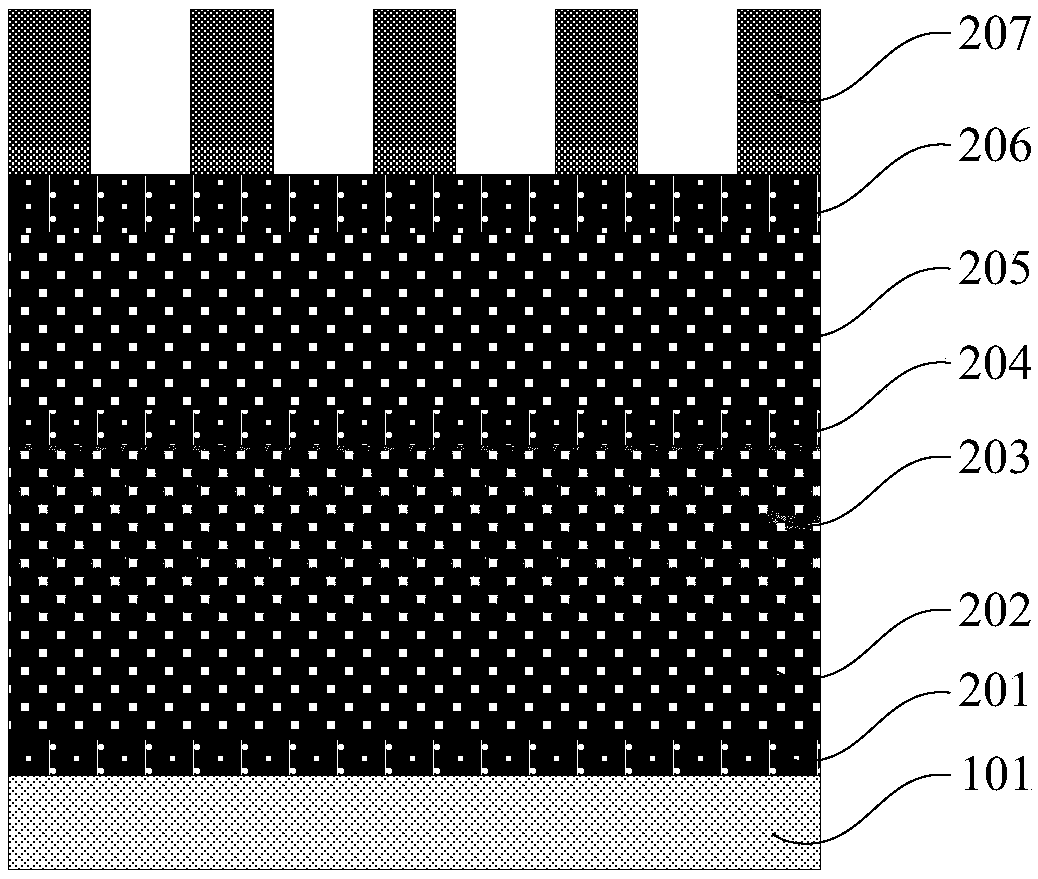
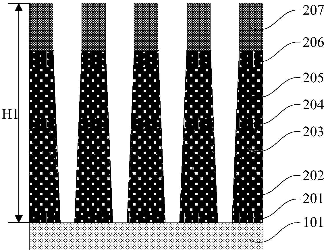
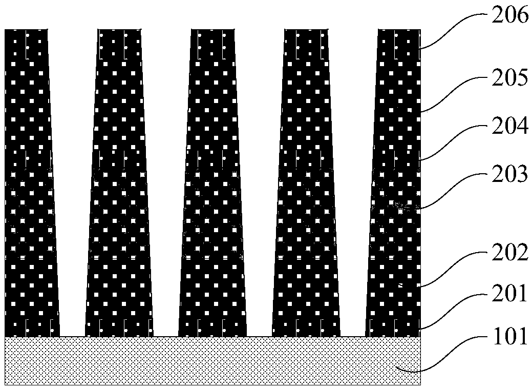
technical field [0001] The invention relates to the technical field of semiconductor integrated circuit manufacturing, in particular to a method for improving the morphology of capacitor holes. Background technique [0002] With the development of semiconductor technology, dynamic random access memory (DRAM) devices are getting smaller and smaller, the aspect ratio of capacitors is getting bigger and bigger, etching is becoming more and more difficult, and the shape control of capacitor holes is becoming more and more difficult. more difficult. [0003] Such as Figure 1-3 As shown, the method for forming capacitor holes in the prior art is shown. Such as figure 1 As shown, an etch stop layer 201, a first capacitor sacrificial oxide layer 202, a second capacitor sacrificial oxide layer 203, a first capacitor supporting layer 204, a third capacitor sacrificial oxide layer 205, and a second capacitor oxide layer 201 are sequentially deposited on a substrate 101. A supporti...
Claims
Application Information
Patent Timeline
Application Date:The date an application was filed.
Publication Date:The date a patent or application was officially published.
First Publication Date:The earliest publication date of a patent with the same application number.
Issue Date:Publication date of the patent grant document.
PCT Entry Date:The Entry date of PCT National Phase.
Estimated Expiry Date:The statutory expiry date of a patent right according to the Patent Law, and it is the longest term of protection that the patent right can achieve without the termination of the patent right due to other reasons(Term extension factor has been taken into account ).
Invalid Date:Actual expiry date is based on effective date or publication date of legal transaction data of invalid patent.
