Nanoimprint structure, control method thereof, nanoimprint apparatus, and patterning method

A technology of nano-imprinting and patterning, applied in the fields of nano-imprinting devices and nano-imprinting structures, can solve the problems of poor quality of soft templates, inability to guarantee uniformity, affecting display quality, etc.

Active Publication Date: 2020-04-10
BOE TECH GRP CO LTD
View PDF7 Cites 0 Cited by
  • Summary
  • Abstract
  • Description
  • Claims
  • Application Information

AI Technical Summary

Problems solved by technology

However, in the process of forming the soft template, each soft film board needs to copy the graphics on the hard template separately, and it cannot be guaranteed that the direction of the grating on the hard template copied each

Method used


Image

  • Nanoimprint structure, control method thereof, nanoimprint apparatus, and patterning method
  • Nanoimprint structure, control method thereof, nanoimprint apparatus, and patterning method
  • Nanoimprint structure, control method thereof, nanoimprint apparatus, and patterning method

Examples


Embodiment Construction

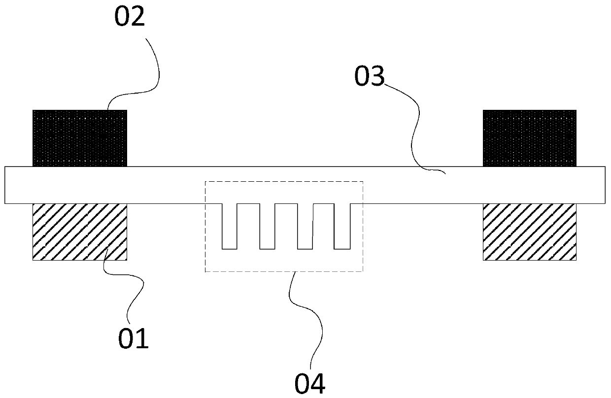
[0040] In the nanoimprint technology in the related art, the hard template is made first, and then the hard template is re-engraved through the soft film plate, and the imprint pattern is formed on the soft template. Among them, because the hard template manufacturing process takes a long time, repeated Only one corresponding hard template is made for the graphics, and the graphics on the hard template are reproduced to different areas through multiple soft film plates, so as to realize the composition of different areas of the substrate.

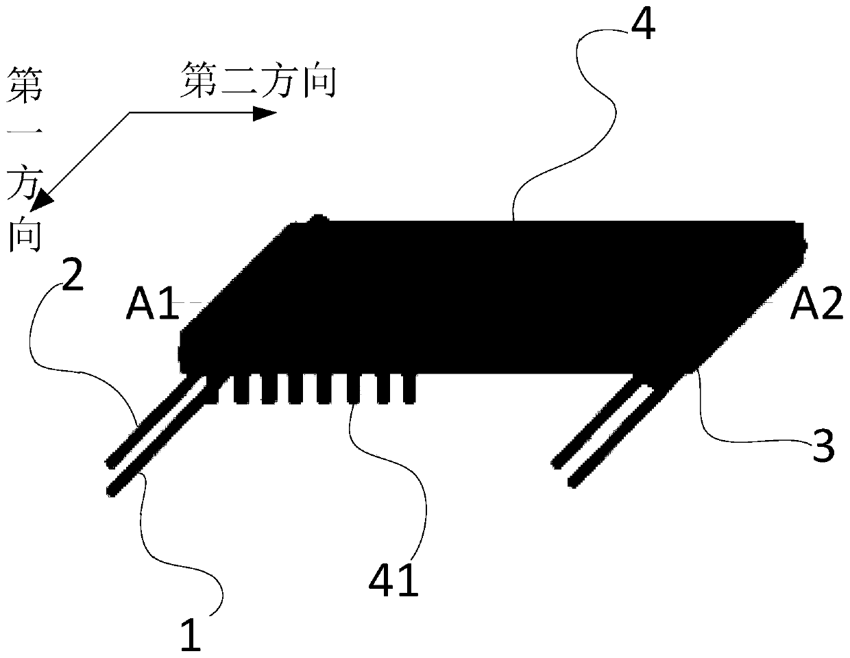
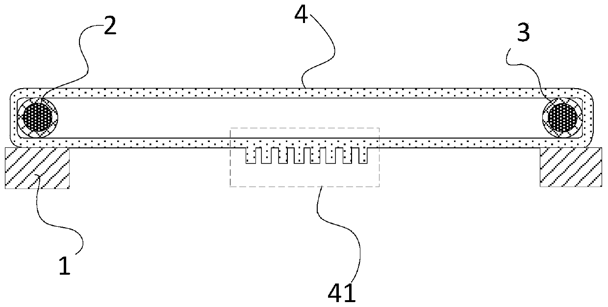
[0041] Among them, nanoimprint structures in related technologies, such as figure 1 As shown, it includes: fixed magnet 01, magnetic connecting rod 02, and the soft membrane plate 03 is fixed between the fixed magnet 01 and the magnetic connecting rod 02 through the suction force between the fixed magnet 01 and the magnetic connecting rod 02, each soft membrane The area where the embossed pattern 04 is located in the plate 03 is not the sam...


PUM

PropertyMeasurementUnit
Extension lengthaaaaaaaaaa

Abstract

The invention discloses a nanoimprint structure, a control method thereof, a nanoimprint device and a composition method. A bearing structure is arranged on a magnetic connecting rod, a soft film plate is arranged to be an annular soft film plate; the annular soft film plate sleeves the position, with the bearing structure, of the magnetic connecting rod; the bearing structure is controlled to rotate around the magnetic connecting rod; the impressing pattern of the annular soft film plate is driven to move in the second direction; the bearing structure is controlled to slide on the magnetic connecting rod; according to the method, the impressing pattern of the annular soft film plate is driven to move in the first direction, so that one annular soft film plate is arranged, the compositionof the substrate can be completed by adjusting the area where the impressing pattern is located, the problem of composition uniformity caused by splicing of multiple soft film plates is solved, and the production cost is greatly saved.

Description

technical field [0001] The invention relates to the field of display technology, in particular to a nanoimprint structure, a control method thereof, a nanoimprint device and a patterning method. Background technique [0002] Using nanoimprint technology for patterning, because it can form nanoscale dimensions, it can make the display panel achieve high resolution, and it also has the advantages of simple process, ultra-low cost, and high productivity. It is widely used in LEDs, semiconductors, etc. The field of micro-nano manufacturing is considered to be one of the promising next-generation lithography technologies. [0003] In the existing nanoimprinting process, due to the limitation of the size of the hard template, the hard template can only be copied multiple times, and multiple soft templates can be copied, so that the position of the embossed pattern in each soft film plate is different. The different positions of the substrate are patterned by the board, so that th...

Claims


Application Information

Patent Timeline
IPC IPC(8): G03F7/00
CPCG03F7/0002
Inventor 周雪原张笑李多辉路彦辉郭康谷新谭伟刘震赵晋
Owner BOE TECH GRP CO LTD
Why Eureka
Try Eureka