A flying shooting method, system, and chip bonding method and system

A chip bonding and chip technology, which is applied to the parts of TV system, TV, color TV, etc., can solve the vibration between the bonding head and the camera, the limited range of the camera to take pictures, and affect the efficiency of chip bonding, etc. problem, achieve the effect of shortening the shutter time, shortening the lighting time, and improving the bonding efficiency

Active Publication Date: 2021-08-31
SHENZHEN DEVOL ADVANCED AUTOMATION CO LTD
View PDF6 Cites 0 Cited by
  • Summary
  • Abstract
  • Description
  • Claims
  • Application Information

AI Technical Summary

Problems solved by technology

[0007] However, the camera has a limited range of pictures, so each time the camera only takes pictures of the chip corresponding to the bonding head, and moves to the next chip after welding to take pictures
[0008] The disadvantages of the existing technology are: when moving to the top of each chip, it is necessary to stop and take pictures before welding, the acceleration of the bonding head from motion to stop is relatively large, and the bonding head and the camera will vibrate, affecting The camera takes pictures, so the camera needs to wait for the vibration to stop before taking pictures. The staying time affects the efficiency of chip bonding

Method used


Image

  • A flying shooting method, system, and chip bonding method and system
  • A flying shooting method, system, and chip bonding method and system
  • A flying shooting method, system, and chip bonding method and system

Examples


Embodiment

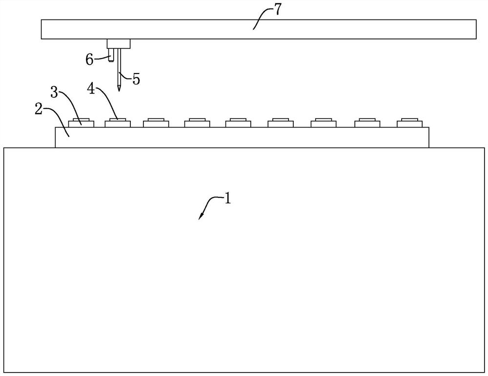
[0038] Embodiment, a kind of LED bonding equipment, refer to figure 1 , including a frame 1, a fixture workbench 2 is fixedly connected to the frame 1, a plurality of fixtures 3 are fixedly connected to the fixture workbench 2, a bonding workbench 7 is arranged above the fixture workbench 2, and the bonding workbench 7 is close to the fixture A bonding head 5 is fixedly connected to one side of the workbench.

[0039] The chip 4 is fixed on the jig 3 , and the chip 4 is welded and bonded through the bonding head 5 .

[0040] The camera 6 with the lens facing the fixture 3 is fixedly connected to the bonding head 5, and the camera 6 is electrically connected to a computer. Path planning is carried out, and the computer controls the bonding head 5 to move according to the specified path, and solders the electronic devices on the chip 4 .

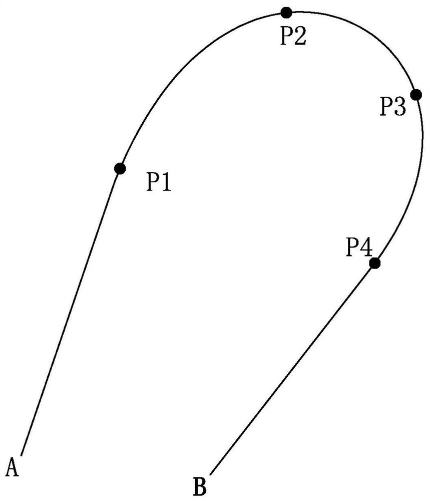
[0041] A kind of bonding method of chip 4, combines figure 2 , image 3 .
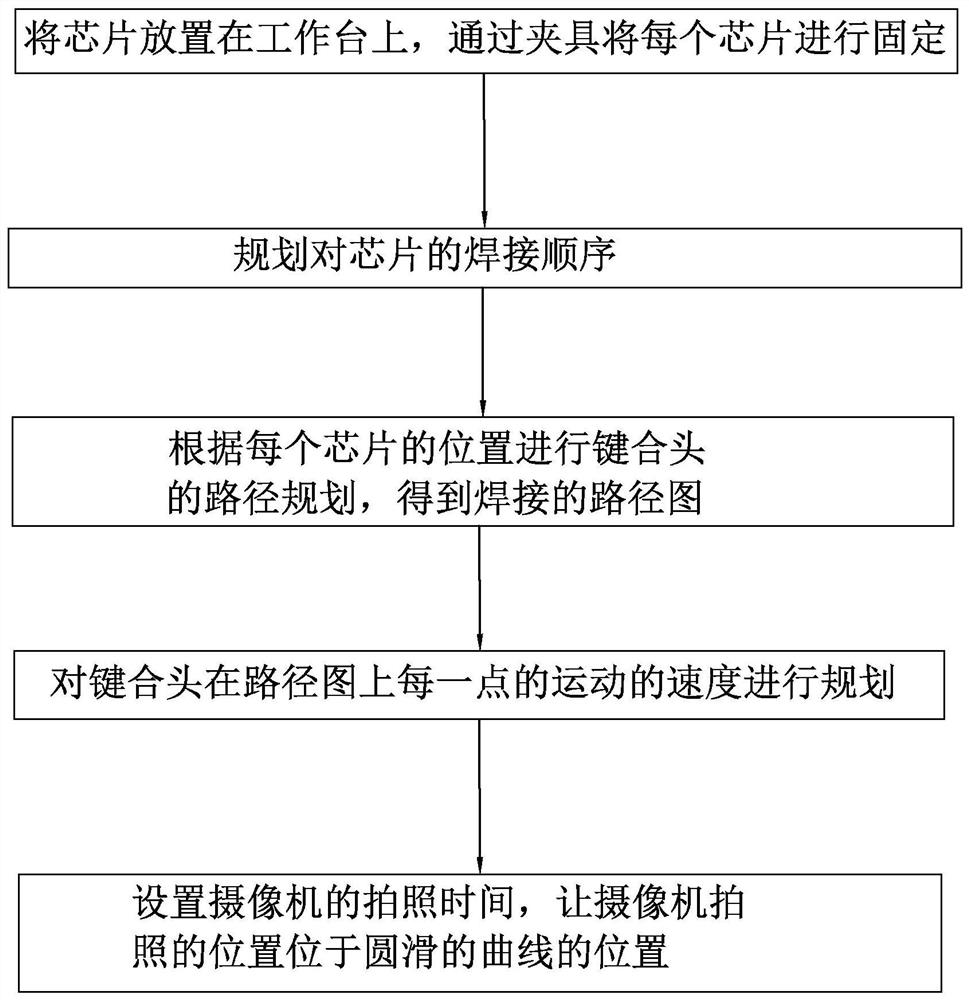
[0042] first step,

[0043] Place the chip 4 on the fixtur...


PUM


Abstract

The invention discloses a flying shooting method and system, and a chip bonding method and system, and relates to the technical field of chip bonding. For the bonding head of the bonded chip, plan the photographing position of each chip according to the position of each chip, plan the movement path of the bonding head, and set the motion path segment where the photographing position is located as a smooth curve. The camera is fixed on the top, and the camera is used to complete the photo. When the camera moves to the photo position, the camera moves at a constant speed. The product of the speed of the camera movement and the camera photo time is less than the pixel length of the photo taken by the camera. The invention improves the precision of the coordination of vision and motion control, reduces the time spent on the coordination of vision and motion control, and has the advantages of improving the precision and efficiency of bonding equipment.

Description

technical field [0001] The present invention relates to the technical field of chip bonding, in particular to a flying shooting method and system, and a chip bonding method and system. Background technique [0002] LED bonding equipment is a key semiconductor equipment that connects chip pads and package pins with metal wires. Its main working principle is: heating and applying ultrasound to the metal wire and the pressure soldering point at the same time, the contact surface will produce plastic deformation and damage The oxide film on the interface activates it and completes the connection through mutual diffusion between the two metals on the contact surface. [0003] refer to figure 1 , in the prior art, the LED bonding equipment includes a workbench, which is provided with a plurality of clamps for tightening the chip, on the workbench is provided with a bonding head for welding electronic devices in the chip, and on the frame is provided with The kinematic mechanism ...

Claims


Application Information

Patent Timeline
Patent Type & Authority Patents(China)
IPC IPC(8): H04N5/232H04N5/235
CPCH04N23/66H04N23/73H04N23/74
Inventor 黎明森程炜张振夺班华志沈宣佐李凤明
Owner SHENZHEN DEVOL ADVANCED AUTOMATION CO LTD
Why Eureka
Try Eureka