IGBT design method
A design method and parameter technology, applied in design optimization/simulation, electrical components, circuits, etc., can solve the problems of long tape-out experiment cycle and high cost, and achieve the effect of shortening the design cycle and design cost
- Summary
- Abstract
- Description
- Claims
- Application Information
AI Technical Summary
Problems solved by technology
Method used
Image
Examples
Embodiment Construction
[0034] In order to make the object, technical solution and advantages of the present invention clearer, the present invention will be further described in detail below in conjunction with the accompanying drawings and embodiments. It should be understood that the specific embodiments described here are only used to explain the present invention, not to limit the present invention.
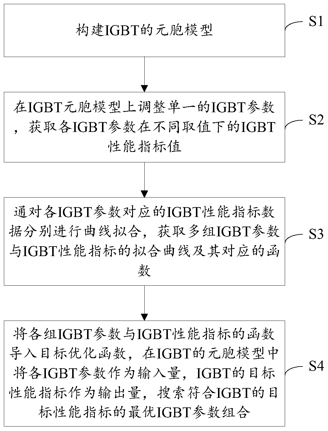
[0035] figure 1 The flowchart of the IGBT design method provided by the embodiment of the present invention, the method specifically includes the following steps:
[0036] S1, constructing the cell model of IGBT;
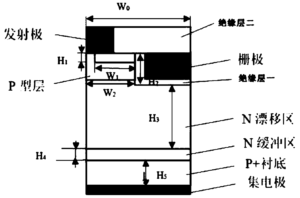
[0037] Using semiconductor device structure and process simulation software to build the IGBT cell structure, the schematic diagram of the IGBT cell structure is as follows figure 2 As shown, from the bottom to the top, the collector, the P+ substrate, the N buffer zone, the N drift region, the P-type layer and the gate arranged in parallel on the N drift region, between the gate and ...
PUM
 Abstract
Description
Claims
Application Information


