Optical film processing method for backlight source, backlight source and mobile terminal

A technology of optical film and processing method, which is applied in the field of backlight, and can solve problems such as poor backlight effect, poor backlight, and wrinkling of the optical film, and achieve the effect of improving the effect of backlight and improving the wrinkling phenomenon

Inactive Publication Date: 2020-05-19
SHENZHEN SOUTH POLE OPTOELECTRONICS TECH
View PDF9 Cites 0 Cited by
  • Summary
  • Abstract
  • Description
  • Claims
  • Application Information

AI Technical Summary

Problems solved by technology

[0004] The optical film will expand and deform after being subjected to high temperature. If the heated area of ​​the optical film is not fully released, it will cause wrinkling and cause poor backlight; the backlight in mobile terminals usually adopts direct backlight or side-in Type backlight, for the direct type backlight, the LED light strip is usually parallel to the short side of the optical film, and the wrinkles generated by the heating of the optical film will spread from one end of the short side to other positions, causing the entire optical Severe wrinkling of the diaphragm, resulting in poor backlight effect

Method used


Image

  • Optical film processing method for backlight source, backlight source and mobile terminal
  • Optical film processing method for backlight source, backlight source and mobile terminal
  • Optical film processing method for backlight source, backlight source and mobile terminal

Examples


Embodiment Construction

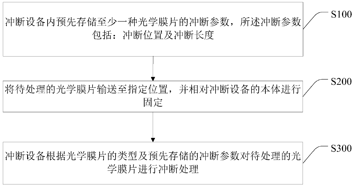
[0028] In order to make the object, technical solution and advantages of the present invention more clear, the present invention will be further described in detail below in conjunction with the accompanying drawings and embodiments. It should be understood that the specific embodiments described here are only used to explain the present invention, not to limit the present invention.

[0029] Such as figure 1 As shown, the present invention provides a kind of optical film processing method for backlight source, and this method is used for punching and processing the optical film film in backlight source, and it comprises steps:

[0030] S100. Pre-store at least one punching parameter of the optical film in the punching device, where the punching parameter includes: a punching position and a punching length.

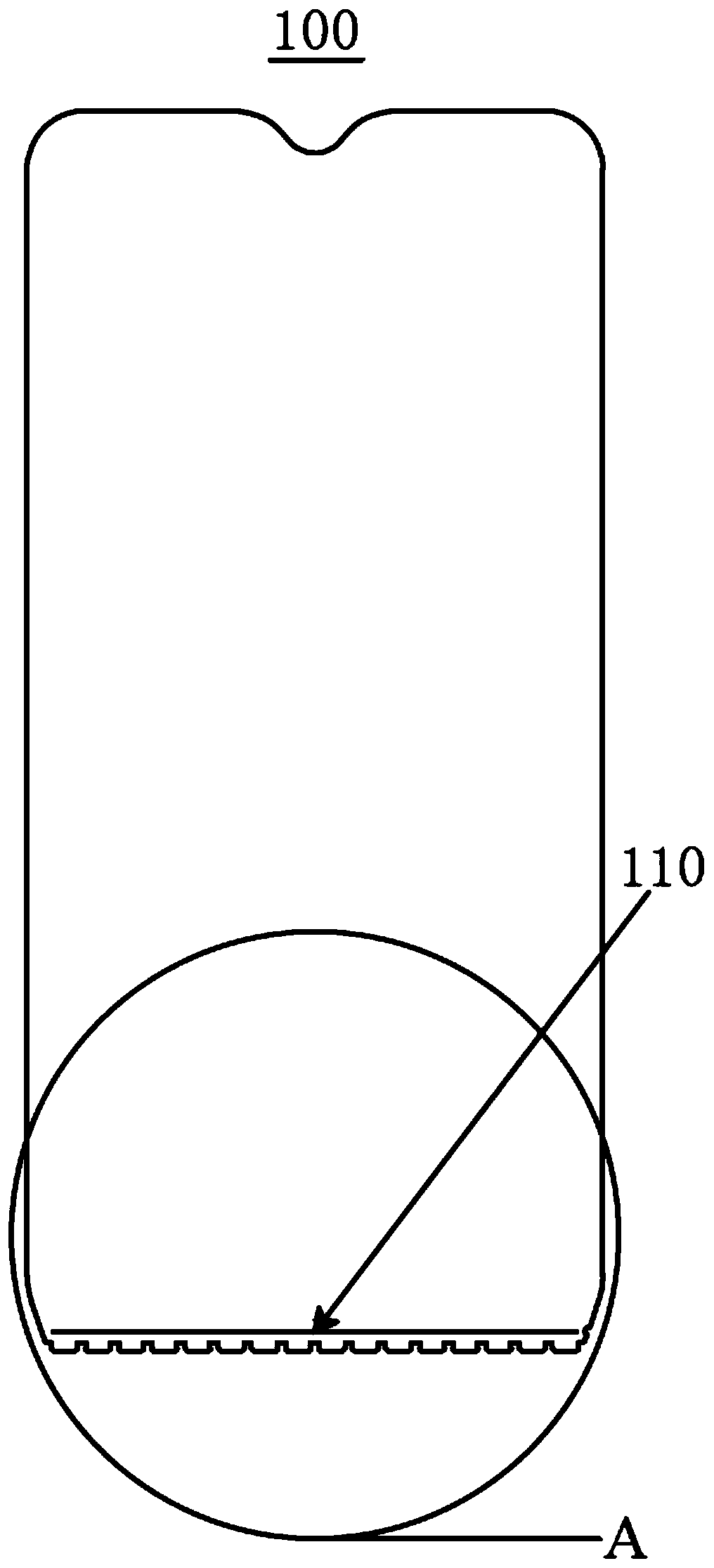
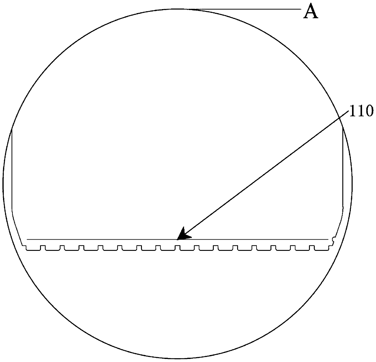
[0031] In a preferred embodiment of the present invention, the optical film includes a reflective film 100, such as figure 2 As shown, the breaking position of the ref...


PUM

PropertyMeasurementUnit
widthaaaaaaaaaa
lengthaaaaaaaaaa
lengthaaaaaaaaaa

Abstract

The invention relates to an optical film processing method for a backlight source, the backlight source and a mobile terminal, and the method comprises the steps: pre-storing the punching parameters of at least one type of optical film in punching equipment, wherein the punching parameters comprise a punching position and a punching length; conveying the optical film to be processed to a specifiedposition, and fixing the optical film relative to the body of the punching equipment; and the punching equipment carries out punching treatment on the to-be-treated optical film according to the typeof the optical film and the pre-stored punching parameters. According to the method, punching treatment is performed on at least one optical film, when the punched optical film is heated to expand, the deformation is stopped at the punching-off position, finally, the punching-off position serves as a parting line, the part, close to the LED lamp strip, of the optical film deforms, the part, awayfrom the LED lamp strip, of the optical film does not deform or only slightly deforms, and thhus the wrinkling phenomenon of the optical film is improved and the backlight effect of the backlight source is improved.

Description

technical field [0001] The present invention relates to the technical field of backlights, in particular to an optical film processing method for backlights, backlights and mobile terminals. Background technique [0002] The backlight (Back Light) is a light source located behind the liquid crystal display (LCD), and its luminous effect will directly affect the visual effect of the liquid crystal display module (LCM). Backlights are widely used in touch screens, backlights, LCD / LCM, mobile phones, tablet computers, GPS and solar cells and other industries; they are mainly composed of light sources, light guide plates, optical modules and structural parts; among them, the light sources mainly include EL, CCFL and LED backlight types; light guide plates are divided into printing, chemical etching (Etching), precision mechanical characterization (V-cut), light lithography (Stamper), internal diffusion, and hot pressing; optical dies: light-enhancing film / sheet, diffusion film...

Claims


Application Information

Patent Timeline
Patent Type & Authority Applications(China)
IPC IPC(8): G02F1/13357
CPCG02F1/133605G02F1/133606
Inventor 徐贤强李良桐姜发明
Owner SHENZHEN SOUTH POLE OPTOELECTRONICS TECH
Why Eureka
Try Eureka