Backlight module, manufacturing method thereof and display device

A technology of backlight module and manufacturing method, which is applied in the direction of electrical components, electric solid devices, circuits, etc., can solve problems such as uneven light mixing of backlight modules, pulling of light-emitting chips, etc., and achieve the effect of reducing leakage and improving uniformity

Active Publication Date: 2020-06-12
BOE TECH GRP CO LTD +1
View PDF9 Cites 11 Cited by
  • Summary
  • Abstract
  • Description
  • Claims
  • Application Information

AI Technical Summary

Problems solved by technology

[0004] The purpose of the present invention is to provide a backlight module and its manufacturing method and display device, which are used to solve the existing problems of the existing backlight module due to the volatilization of flux and solvent in the solder paste and the easy melting of the solder paste during the reflow soldering process. The pulling of the light-emitting chip will cause the light-emitting chip placed on the solder paste to tilt, so that the light-emitting chip will form a certain angle with the surface of the substrate, which will cause local or large-area uneven light mixing in the backlight module.

Method used


Image

  • Backlight module, manufacturing method thereof and display device
  • Backlight module, manufacturing method thereof and display device
  • Backlight module, manufacturing method thereof and display device

Examples


Embodiment Construction

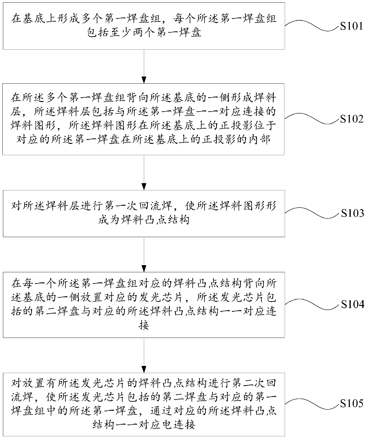
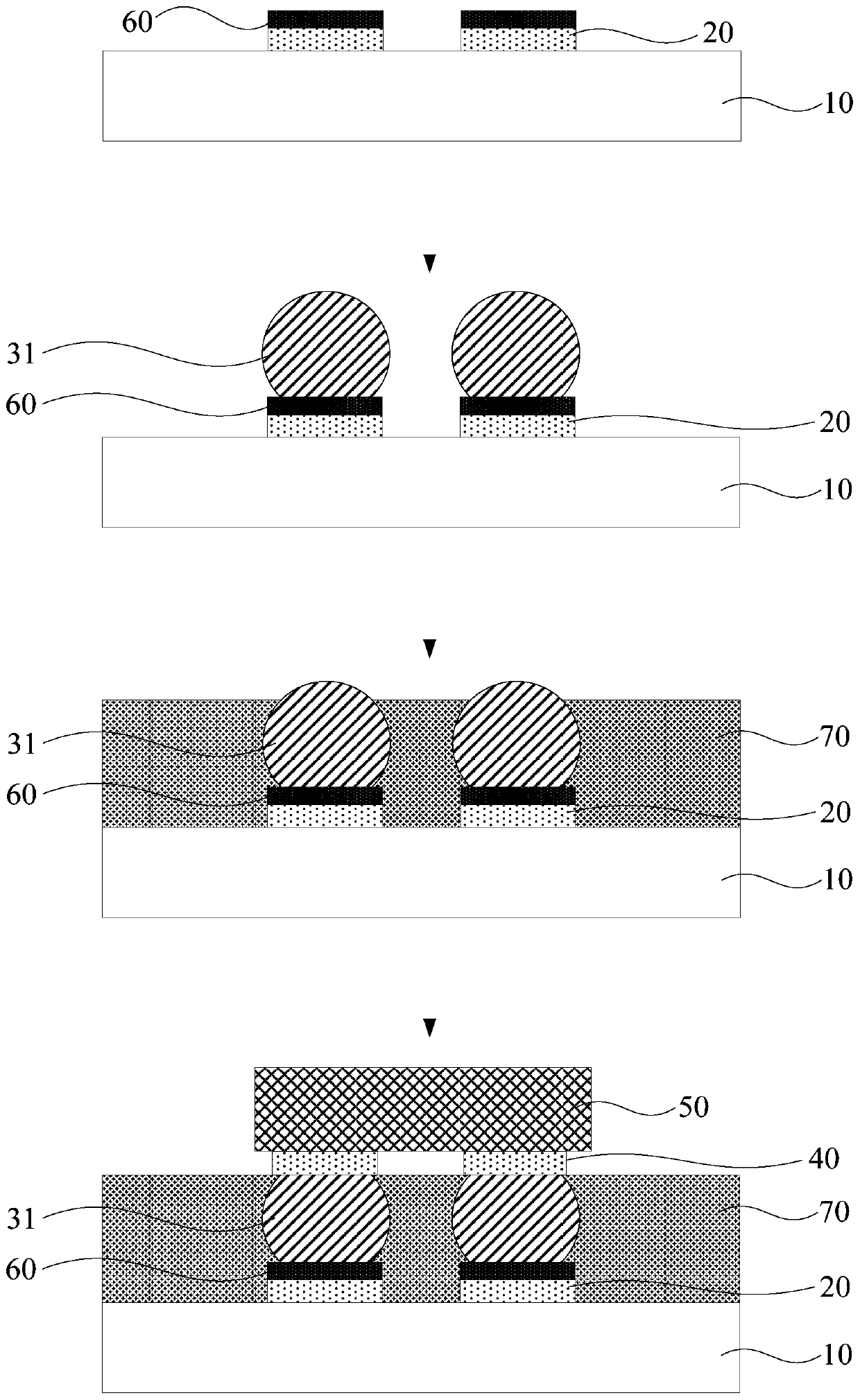
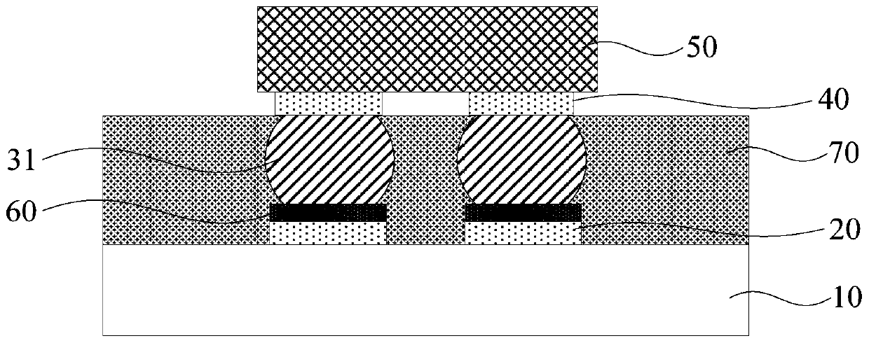
[0043] In order to further illustrate the backlight module, its manufacturing method, and display device provided by the embodiments of the present invention, a detailed description will be given below in conjunction with the accompanying drawings.

[0044] In the related art, when Mini LED is used as the light source structure in the backlight module, the number of Mini LED used in the backlight module is increasing, and as the size of the Mini LED chip is continuously reduced, it is difficult to make the backlight module. The difficulty of the process puts forward higher requirements.

[0045] When making traditional miniature light-emitting diode (Mini LED) backlight modules, first print solder paste on the substrate, then place the Mini LED chip on the printed solder paste, and then fix the Mini LED chip on the substrate through a reflow process. However, this production method currently has the following problems:

[0046] (1) In the traditional solder paste printing pro...


PUM


Abstract

The invention provides a backlight module, a manufacturing method thereof and a display device, relates to the technical field of display, and aims to solve the problem of uneven local or large-area light mixing of an existing backlight module. The manufacturing method of the backlight module comprises the following steps: forming a plurality of first bonding pad groups on a substrate, wherein each first bonding pad group comprises at least two first bonding pads; forming a solder layer, wherein the solder layer comprises solder patterns connected with the first bonding pads in a one-to-one correspondence manner; performing reflow soldering for the first time to enable the solder pattern to form a solder bump structure; placing a corresponding light-emitting chip on one side, back to the substrate, of the solder bump structure corresponding to each first bonding pad group, wherein second bonding pads included in the light-emitting chip are connected with the corresponding solder bump structures in a one-to-one correspondence manner; and performing reflow soldering for the second time, so that the second bonding pads included in the light-emitting chip are electrically connected with the corresponding first bonding pads in a one-to-one correspondence manner through the corresponding solder bump structures. The manufacturing method of the backlight module is used for manufacturing the backlight module.

Description

technical field [0001] The invention relates to the field of display technology, in particular to a backlight module, a manufacturing method thereof, and a display device. Background technique [0002] The traditional miniature light-emitting diode (Mini LED) backlight module mainly includes a substrate and Mini LED chips arrayed on the substrate. When making the backlight module, solder paste is first printed on the substrate, and then the Mini LED chips are placed on the printed surface. On the solder paste, and then through the reflow process, the Mini LED chip is fixed on the substrate. [0003] However, in the reflow soldering process, the volatilization of flux and solvent in the solder paste and the melting of the solder paste can easily cause the pulling of the light-emitting chip, which makes the light-emitting chip placed on the solder paste tilt, so that the light-emitting chip and the surface of the substrate form a certain angle. , resulting in partial or large...

Claims


Application Information

Patent Timeline
Patent Type & Authority Applications(China)
IPC IPC(8): H01L25/075H01L33/62
CPCH01L25/0753H01L33/62H01L2933/0066
Inventor 熊志军马俊杰初宇天卢元达岂林霞翟明
Owner BOE TECH GRP CO LTD
Why Eureka
Try Eureka