
Chip pin clamp and chip pin clamp array

A chip and pin technology, applied in the field of chip pin fixtures and chip pin fixture arrays, can solve problems such as low efficiency, random impedance of conductive parts, damage to circuit boards or chip pins, etc., to reduce stress and ensure use The effect of longevity

Active Publication Date: 2020-07-03
中昊芯英(杭州)科技有限公司
View PDF6 Cites 2 Cited by
  • Summary
  • Abstract
  • Description
  • Claims
  • Application Information

AI Technical Summary

Problems solved by technology

Use a multimeter to detect the chip pins that have been soldered to the circuit board. Due to the difficulty in positioning, it is easy to cause irreversible physical damage to the circuit board or chip pins. At the same time, the multimeter cannot diagnose the transient response of the analog circuit, and the usage scenarios are very limited; oscilloscopes and other parallel connections The degree of freedom of the diagnostic tool for accessing the circuit is very limited, it is impossible to detect multiple pins at the same time, and each time the target pin for detection is changed, rewiring is required, which is inefficient
If an adapter board is used for multi-pin detection, it is necessary to customize multiple sets of different adapter boards for chips with different pin numbers or structures, which is expensive, and after the adapter board is reused many times, the conductive parts in it will be damaged. Easy to generate random impedance, causing diagnostic errors

Method used


Image

  • Chip pin clamp and chip pin clamp array
  • Chip pin clamp and chip pin clamp array
  • Chip pin clamp and chip pin clamp array

Examples


Embodiment Construction

[0032] The following will clearly and completely describe the technical solutions in the embodiments of the present invention with reference to the accompanying drawings in the embodiments of the present invention. Obviously, the described embodiments are only some, not all, embodiments of the present invention. Based on the embodiments of the present invention, all other embodiments obtained by persons of ordinary skill in the art without making creative efforts belong to the protection scope of the present invention.

[0033]The terms "first", "second" and the like in the description and claims of the present invention and the drawings are used to distinguish different objects, rather than to describe a specific order. The terms "upper", "lower", "left", "right", "top", and "bottom" only represent relative positional relationships, rather than specific spatial limitations. The term "at least one" means one or more than one, and the term "plurality" means two or more, unless ...


PUM


Abstract

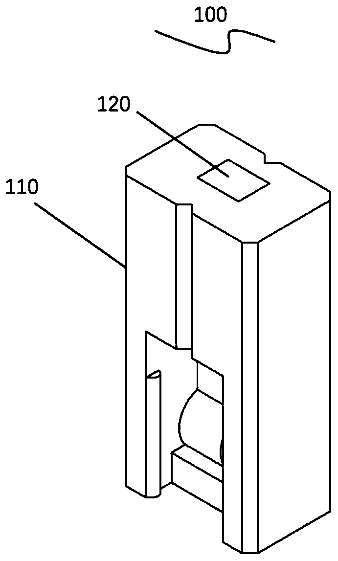
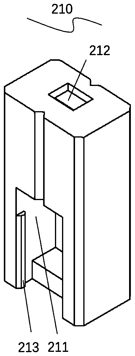
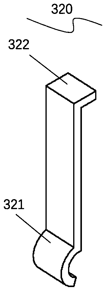
The invention provides a chip pin clamp and a chip pin clamp array. The chip pin clamp comprises an insulating shell and a conductive elastic piece, based on a structure of the shell, the chip pin clamp can be stably and reliably clamped on a chip pin, at the moment, a contact part of the elastic piece makes contact with a chip pin to achieve conduction, the elastic piece is connected with external equipment through a switching part of the elastic piece, and therefore detection or external signal input of the chip pin is achieved. The chip pin clamp is advantaged in that the chip pin clamp array provided by the invention can cover detection requirements of chips with different numbers of pins, and efficiently and conveniently realizes multi-pin measurement and signal input.

Description

technical field [0001] The invention relates to the field of integrated circuits, in particular to a chip pin clamp and a chip pin clamp array. Background technique [0002] The circuit board is one of the indispensable basic circuit components in electronic products, and has been widely used in various fields such as industrial control and artificial intelligence. In order to ensure the stable operation of the circuit board, it is necessary to detect the chip soldered in the circuit board, that is, to detect or monitor the actual working conditions of the chip pins. [0003] Commonly used techniques for detecting chip pins include direct diagnosis of chip pins using diagnostic tools such as multimeters and oscilloscopes. Using a multimeter to detect the chip pins that have been soldered to the circuit board, due to the difficulty in positioning, it is easy to cause irreversible physical damage to the circuit board or chip pins. At the same time, the multimeter cannot diagn...

Claims


Application Information

Patent Timeline
IPC IPC(8): G01R1/04G01R31/28
CPCG01R1/0425G01R31/2886
Inventor 王博赟杨龚轶凡郑瀚寻闯小明
Owner 中昊芯英(杭州)科技有限公司
Learn More