
Chip automatic verification system and method therefor

An automatic verification and chip technology, applied in the field of verification platform, can solve the problems of increasing verification error rate, labor-intensive, time-consuming, etc.

Active Publication Date: 2020-07-07
NUVOTON
View PDF8 Cites 0 Cited by
  • Summary
  • Abstract
  • Description
  • Claims
  • Application Information

AI Technical Summary

Problems solved by technology

[0004] However, using pulse width, cycle time or duty cycle to decode signals is very time-consuming and labor-intensive in circuit verification, because engineers must manually input preset test parameters into the device under test
[0005] In addition, in the system verilog environment under the framework of the existing Universal Verification Methodology (Universal Verification Methodology), the verification method can only be manually compared with one-to-one output signals of the circuit under test. If a large number of random input signals are encountered , will make the output signal very complex and increase the verification error rate

Method used


Image

  • Chip automatic verification system and method therefor
  • Chip automatic verification system and method therefor
  • Chip automatic verification system and method therefor

Examples


Embodiment Construction

[0037] Embodiments of the present invention will be described below in conjunction with related figures. In the drawings, the same symbols represent the same or similar elements or method flows.

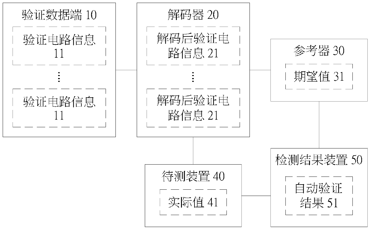
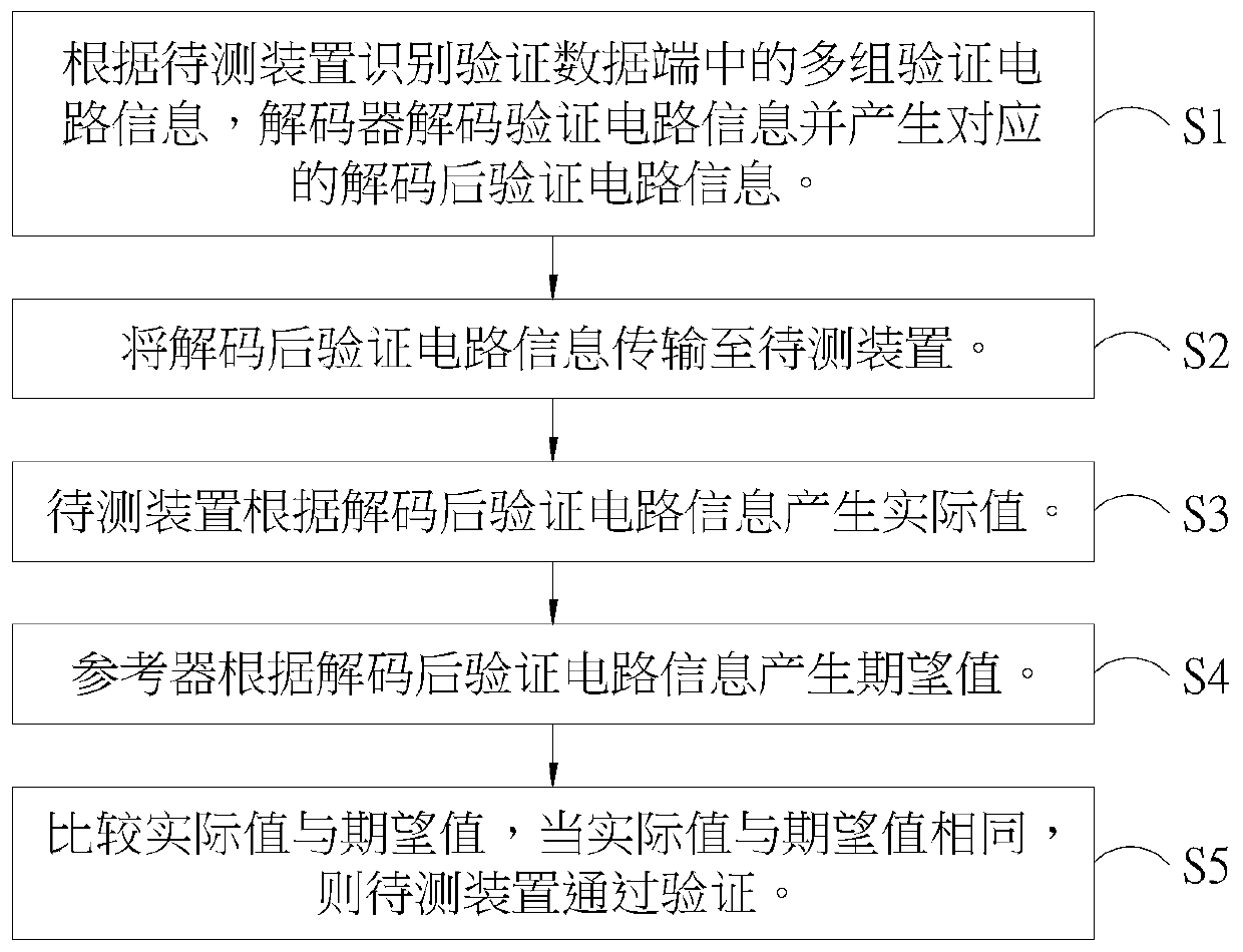
[0038] Please refer to figure 1 , which is an automatic chip verification system for verifying the signal of the device under test, which includes a verification data terminal 10 , a decoder 20 , a reference device 30 and a test result device 50 . The verification data terminal 10 stores multiple sets of verification circuit information 11 . The decoder 20 is connected to the verification data terminal 10, and decoded according to at least one verification circuit information 11 to generate at least one corresponding decoded verification circuit information 21. The decoder 20 is connected to the device under test 40, and the device under test 40 is verified according to the decoded verification circuit information. The information 21 produces an actual value 41 . The reference dev...


PUM


Abstract

The invention provides a chip automatic verification system, which is used for verifying the signal of the device under test. The system includes a verification data terminal, a decoder, a reference device and a detection result device. The verification data terminal stores multiple sets of verification circuit information. The decoder is connected to the verification data terminal, and decodes atleast one verification circuit information to generate corresponding at least one decoded verification circuit information; the decoder is connected with the device under test so that the device under test generates actual values according to the decoded verification circuit information. The reference device is connected with the decoder and generates the expected value according to the information of the verification circuit after decoding. The detection result device is connected with the reference device and the device to be tested. The detection result device outputs the automatic verification result of the signal of the device under test according to the expected value and the actual value.

Description

technical field [0001] The invention relates to a verification platform for automatic detection and verification of any output signal of a single line output circuit (One Wire Output Circuit) based on a universal verification methodology (Universal Verification Methodology) framework. Background technique [0002] After the chip is designed, the verification test can help the designer to detect the designed chip problems. As the current chip architecture is becoming more and more complex, and the types of verification circuits required are also increasing, the time spent on verification and the error rate are also decreasing. increase accordingly. [0003] In the past verification method, engineers need to manually calculate the expected value of each verification characteristic according to the characteristics of the circuit to be verified and verify each parameter. For example, many circuits currently use pulse width, cycle time or duty Cycle is a signal with valid inform...

Claims


Application Information

Patent Timeline
IPC IPC(8): G01R31/28
CPCG01R31/2851G01R31/2834
Inventor 谢景文
Owner NUVOTON
Learn More