Three-dimensional memory device and manufacturing method thereof

A three-dimensional storage and device technology, applied in semiconductor devices, electrical solid devices, electrical components, etc., can solve problems such as incomplete etching of Die edges, and achieve the effect of avoiding incomplete etching and alleviating local stress problems

Active Publication Date: 2020-07-10
YANGTZE MEMORY TECH CO LTD
View PDF6 Cites 10 Cited by
  • Summary
  • Abstract
  • Description
  • Claims
  • Application Information

AI Technical Summary

Problems solved by technology

[0004] The object of the present invention is to provide a three-dimensional memory device and its manufacturing method, aiming at solving the risk of incomplete etching of Die edge caused by the load effect of etching, and alleviating the edge The local stress problem and local superposition phenomenon at

Method used


Image

  • Three-dimensional memory device and manufacturing method thereof
  • Three-dimensional memory device and manufacturing method thereof
  • Three-dimensional memory device and manufacturing method thereof

Examples


Embodiment Construction

[0031] The following will clearly and completely describe the technical solutions in the embodiments of the present invention with reference to the drawings in the embodiments of the present invention. Apparently, the described embodiments are only some of the embodiments of the present invention, but not all of them. Based on the embodiments of the present invention, all other embodiments obtained by those skilled in the art without making creative efforts belong to the protection scope of the present invention.

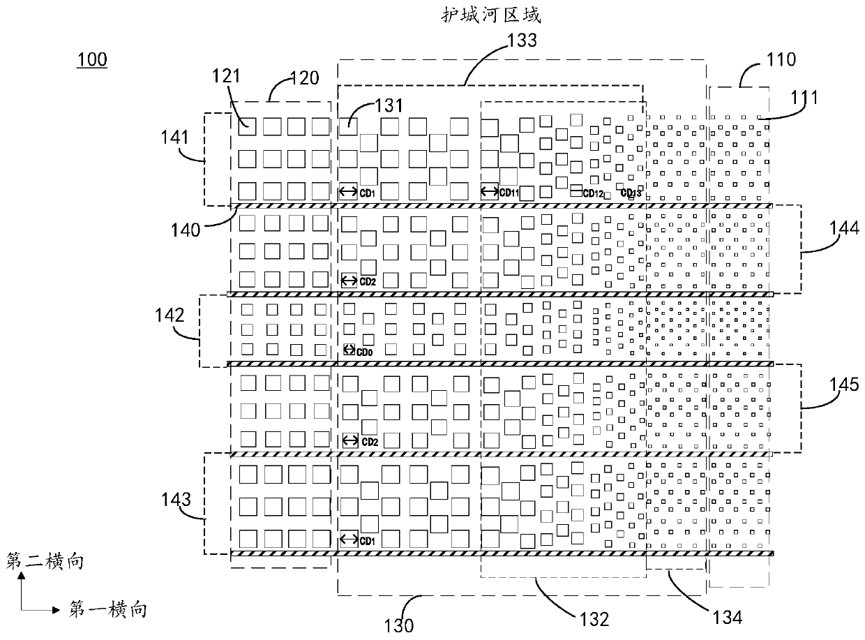
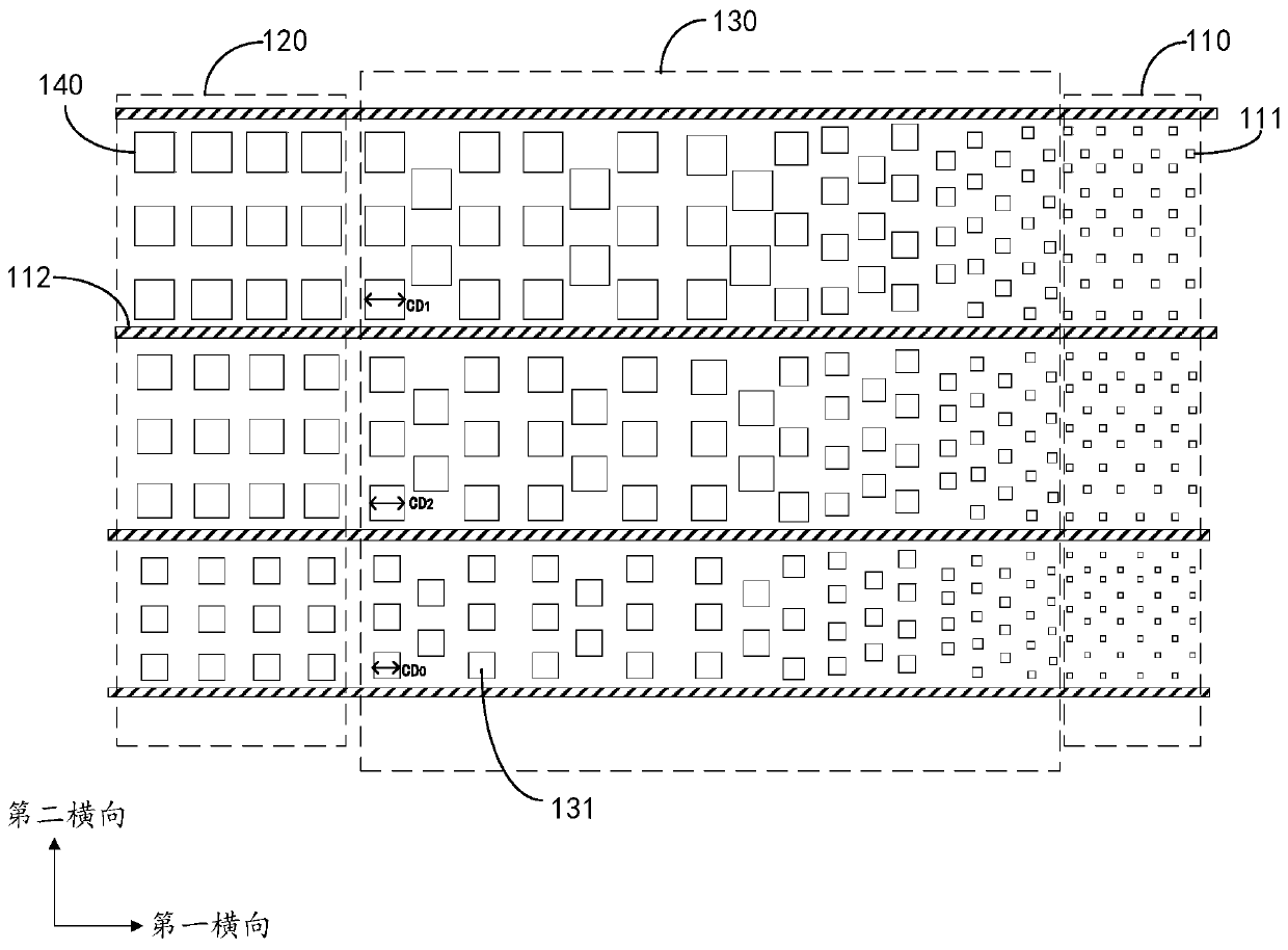
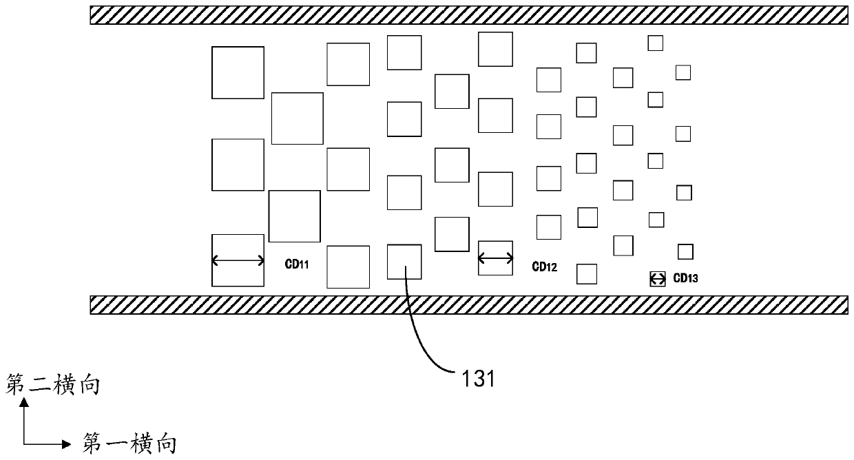
[0032] As used herein, the term "first longitudinal direction" is the Z-axis direction, "first transverse direction" is the X direction, and "second transverse direction" is the Y direction. The term "substrate" refers to the material on which subsequent layers of material are added. The substrate itself can be patterned. Materials added on top of the substrate can be patterned or can remain unpatterned. In addition, the substrate may include various semiconducto...


PUM


Abstract

The invention discloses a three-dimensional memory device and a manufacturing method thereof. The semiconductor device comprises a substrate, a stacking layer, a storage channel array which penetratesthrough the stacking layer in a first longitudinal direction, a grid line slit, a step contact array and a junction region device array, the junction region device array is positioned between the storage channel array and the step contact array; the grid line slit extends in a first transverse direction parallel to the substrate; wherein the junction area device array comprises a plurality of devices; along the second transverse direction, the second transverse direction comprises a first part and a second part; wherein the first edge area and the second edge area are located on the two sidesof the middle area. The critical dimension of the device in the middle region is smaller than the critical dimensions of the first edge region and the second edge region, so that the critical dimension of the device is set to be gradually changed in the second transverse direction, the problem of local stress at the edge can be relieved, and meanwhile, the risk of incomplete channel etching is avoided.

Description

technical field [0001] The invention relates to the technical field of semiconductors and a manufacturing method thereof, in particular to a three-dimensional storage device and a manufacturing method thereof. Background technique [0002] In order to overcome the limitations of two-dimensional memory devices, the industry has developed memory devices having a three-dimensional (3D) structure, which improves integration density by three-dimensionally arranging memory cells over a substrate. [0003] For example, in a three-dimensional memory of 3D NAND flash memory, it usually includes a core area and a step area, and both the core area and the step area may further include various devices. At the edge of the bare chip (Die), from the edge to the middle area, the variation of the pattern density will cause local stress and the risk of incomplete etching. Contents of the invention [0004] The purpose of the present invention is to provide a three-dimensional memory device...

Claims


Application Information

Patent Timeline
Patent Type & Authority Applications(China)
IPC IPC(8): H01L27/11565H01L27/1157H01L27/11582
CPCH10B43/10H10B43/35H10B43/27
Inventor 张富山曾凡清周文斌王恩博阳涵董明张若芳
Owner YANGTZE MEMORY TECH CO LTD
Why Eureka
Try Eureka