Check patentability & draft patents in minutes with Patsnap Eureka AI!

Wafer defect detection method and device

A defect detection and wafer technology, used in measurement devices, semiconductor/solid-state device testing/measurement, material analysis by optical means, etc., can solve the problem of providing optimal focal length conditions for different circuit layout areas, and cannot adapt to different at the same time. The focal length requirements of the circuit layout area, the difficulty of achieving simultaneous focus in different circuit layout areas, etc.

Pending Publication Date: 2020-07-17
NEXCHIP SEMICON CO LTD
View PDF10 Cites 0 Cited by
  • Summary
  • Abstract
  • Description
  • Claims
  • Application Information

AI Technical Summary

Problems solved by technology

[0005] In view of the above problems, the purpose of the present invention is to provide a wafer defect detection method and its device, through the design of the non-rectangular detection area in the defect detection process, to solve the problem of the existing rectangular detection area for different circuit layout areas. It is difficult to achieve the focal length condition of simultaneous focusing, cannot adapt to the focal length requirements of different circuit layout areas at the same time, and cannot give the best focal length conditions for different circuit layout areas

Method used


Image

  • Wafer defect detection method and device
  • Wafer defect detection method and device
  • Wafer defect detection method and device

Examples


Embodiment Construction

[0031] The following will clearly and completely describe the technical solutions in the embodiments of the present invention with reference to the accompanying drawings in the embodiments of the present invention. Obviously, the described embodiments are only some, not all, embodiments of the present invention. Based on the embodiments of the present invention, all other embodiments obtained by persons of ordinary skill in the art without creative efforts fall within the protection scope of the present invention.

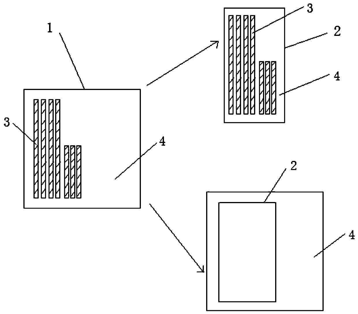
[0032] In the manufacturing process of semiconductor devices, the quality of photolithography is very important, which directly affects the performance, yield and reliability of devices. Generally, there are the following requirements for lithography: the obtained graphics have good integrity, accurate dimensions, neat edges, steep lines, no pinholes in the graphics, no small islands outside the graphics, no dyeing, clean substrate surface, no bottom film and graphi...


PUM


Abstract

The invention discloses a wafer defect detection method and device, and belongs to the technical field of wafer detection. The detection method comprises the following steps: forming a corresponding graph according to a circuit layout area to be detected; according to the graph, obtaining an area conforming to the graph on the wafer, and setting the area as a wafer to-be-detected area of the corresponding circuit layout area; setting at least one detection parameter according to the different circuit layout areas; detecting a wafer to-be-detected area of the circuit layout area according to the at least one detection parameter; and judging whether a wafer defect area exists in the wafer to-be-detected area of the circuit layout area or not according to a preset judgment method. According to the invention, the problem that the existing rectangular detection area is difficult to reach the focal length condition of simultaneous focusing for different circuit layout areas is solved.

Description

technical field [0001] The invention belongs to the technical field of wafer detection, and in particular relates to a wafer defect detection method and a device thereof. Background technique [0002] In the manufacturing process of semiconductor devices, the quality of photolithography is very important, which directly affects the performance, yield and reliability of devices. Generally, there are the following requirements for lithographic wafers: the obtained graphics have good integrity, accurate dimensions, neat edges, steep lines, no pinholes in the graphics, no small islands outside the graphics, no dyeing, clean silicon wafer surface, and no bottom Film and graphic overlays are accurate. [0003] In the detection of wafer defects, digital image processing technology is a relatively common technical form, which can perform specific calculations through sampling and amplitude quantified images, combined with computer information technology and related algorithms, whic...

Claims


Application Information

Patent Timeline
IPC IPC(8): G01N21/956H01L21/66
CPCG01N21/95607H01L22/12H01L22/20G01N2021/95615G01N2021/888G01N2021/8887
Inventor 丁百龙蔡俊郎李发君
Owner NEXCHIP SEMICON CO LTD
Features
  • R&D
  • Intellectual Property
  • Life Sciences
  • Materials
  • Tech Scout
  • Unparalleled Data Quality
  • Higher Quality Content
  • 60% Fewer Hallucinations
Learn More