How to make led display module

A technology of LED display screen and manufacturing method, which is applied in the direction of semiconductor devices, electrical components, circuits, etc., which can solve the problems of poor uniformity of ink color of laminated film layer, etc., and achieve the effect of high ink color consistency and high uniformity

Active Publication Date: 2022-03-18
HCP TECH CO LTD
View PDF9 Cites 0 Cited by
  • Summary
  • Abstract
  • Description
  • Claims
  • Application Information

AI Technical Summary

Problems solved by technology

[0005] In view of the above-mentioned shortcomings of the prior art, the object of the present invention is to provide a method for manufacturing an LED display module, which is used to solve the problem of the uniformity and ink color consistency of the laminated film layer of the LED display module in the prior art. bad question

Method used


Image

  • How to make led display module
  • How to make led display module
  • How to make led display module

Examples


Embodiment 1

[0042] Such as Figure 1 ~ Figure 3 and Figure 8 ~ Figure 10 As shown, the present embodiment provides a method for manufacturing an LED display module, and the method includes:

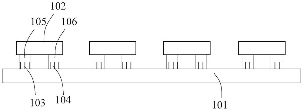
[0043] Such as figure 1 As shown, step 1) is first performed, providing a PCB substrate or glass substrate 101 , and flip-chiping the Mini LED chip 102 on the PCB substrate or glass substrate 101 .

[0044]The PCB substrate or glass substrate 101 includes a first surface and a second surface, the first surface is formed with electrodes for connecting with the Mini LED chip 102, and the second surface has a connecting portion for connecting with the driver chip . The PCB substrate or glass substrate 101 can be a single-layer or multilayer board, and there are interconnection lines inside the PCB substrate or glass substrate 101, and the electrodes include a first electrode 103 and a second electrode 104, and the first electrode 103 can be Positive or negative, the second electrode 104 can be nega...

Embodiment 2

[0056] Such as Figure 1~2 , Figure 4 and Figure 8 ~ Figure 10 As shown, this embodiment provides a method for manufacturing an LED display module, the basic steps of which are as in Embodiment 1, where the difference from Embodiment 1 lies in:

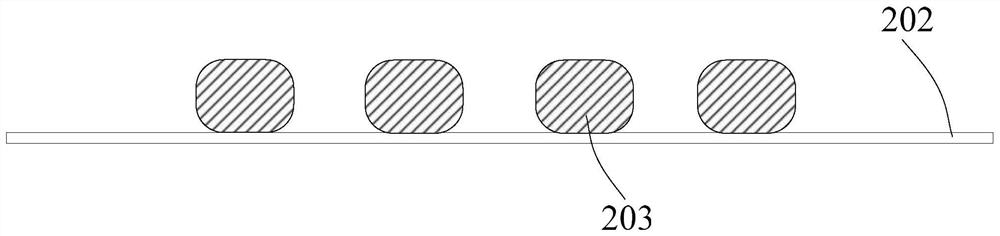
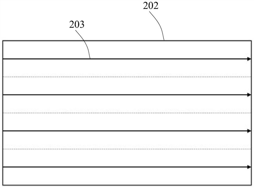
[0057] The shape of the dispersed-coated laminated film material 203 is a line segment array pattern, and the line segment array pattern is a plurality of interlaced line segments in a net shape.

[0058] In a specific implementation process, the line segment array pattern is a plurality of line segments interlaced in a rectangular network, such as Figure 4 As shown, the coating area is divided into several equal sub-regions in the horizontal and vertical directions, such as m parts in the horizontal direction, m≥1, n parts in the vertical direction, n≥1, m and n may or may not be equal. A glue applicator is used to coat the lamination material 203 in the transverse direction, and the coating path is a straight line connecting t...

Embodiment 3

[0060] Such as Figure 1~2 , Figure 5 and Figure 8 ~ Figure 10 As shown, this embodiment provides a method for manufacturing an LED display module, the basic steps of which are as in Embodiment 1, where the difference from Embodiment 1 lies in:

[0061] The shape of the dispersed-coated lamination material 203 is a line segment array pattern, and the line segment array pattern is a spirally bent line segment.

[0062] In a specific implementation process, such as Figure 5 As shown, starting from the center of the coating area, the lamination material 203 is coated spirally to the periphery. The pressure film material 203 can also be coated in a spiral shape from the periphery to the center point of the coating area. In the process of coating the pressing film material 203, the glue amount of the pressing film material 203 can be adjusted according to the position of the spiral part, for example, the amount of the pressing film material 203 located in the central area of...


PUM


Abstract

The present invention provides a method of making LED display modules, including steps: 1) Pour the MINI LED chip on the PCB or glass substrate; 2) one -type membrane, coating the compressive membrane material on the ionized membrane,, Differential coating of the compressive membrane material on the iconic membrane; 3) the coating area of the lyric membrane and the groove body, and the PCB or glass substrate with a MINI LED chip will be out of the coating area with the side of the coating area.The membrane is pressed into the groove body, and the iconic membrane co -shaped fit the groove, and the membrane material is paved around and covered with the mini LED chip;Through the coating method of novel film compressive materials, the invention makes the compressive material scattered as much as possible before the film compression, and the film compression material is scattered on a small area. In the endThe top has high uniformity, so that the LED display module has high ink color consistency.

Description

technical field [0001] The invention belongs to the field of semiconductor display design and manufacture, in particular to a method for manufacturing an LED display module. Background technique [0002] At present, with the development of LED display screens, LED display screens are gradually being used in various fields. With the innovation and development of LED display technology, the small-pitch seamless connection LED display module with high resolution per unit area has become the mainstream product of LED display. It can display higher-definition graphic images and videos, and can also Display more video and image screens, especially in the application of image stitching, which can be seamless and arbitrarily large-area stitching. [0003] The LED display module is one of the main components that make up the finished LED display. At present, the production methods of small-pitch display modules are as follows: 1. Discrete device (SMD); 2. 4-in-1 Mini LED (IMD); 3. ...

Claims


Application Information

Patent Timeline
Patent Type & Authority Patents(China)
IPC IPC(8): H01L33/52H01L25/075
CPCH01L33/52H01L25/0753H01L2933/005
Inventor 庄文荣孙明付小朝黄志强高梓原卢敬权
Owner HCP TECH CO LTD
Why Eureka
Try Eureka