LED chip, display screen module and display screen

A LED chip and display technology, applied in optics, instruments, electrical components, etc., can solve the problems of low brightness ink color consistency, long calibration time, and heavy sorting workload on the display screen, achieve good ink color consistency, reduce Brightness, the effect of reducing light emission

Pending Publication Date: 2022-01-25
东莞市中晶半导体科技有限公司
View PDF0 Cites 0 Cited by
  • Summary
  • Abstract
  • Description
  • Claims
  • Application Information

AI Technical Summary

Problems solved by technology

[0006] In view of the above-mentioned shortcomings of the prior art, the object of the present invention is to provide an LED chip, a display module and a display screen, which are used to solve the problem of large sorting workload and correction problems caused by the high brightness of LED chips in the prior art. Problems of long time, low display brightness and poor ink color consistency

Method used


Image

  • LED chip, display screen module and display screen
  • LED chip, display screen module and display screen
  • LED chip, display screen module and display screen

Examples


Embodiment 1

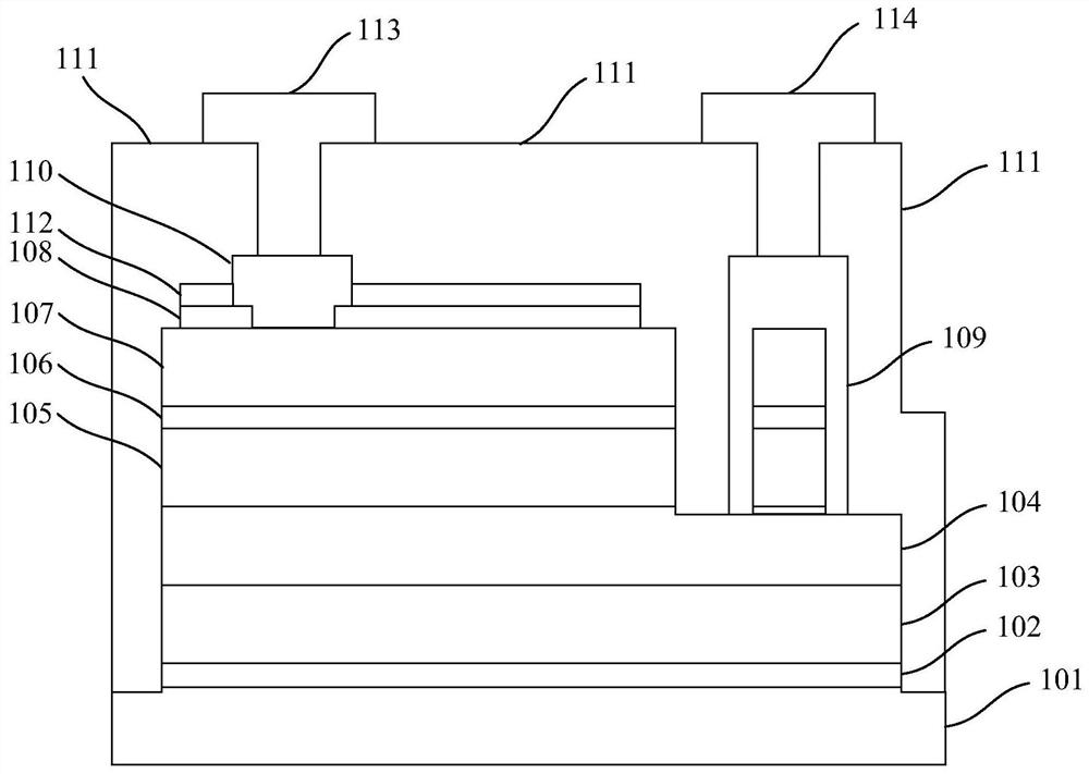
[0051] Such as figure 1 As shown, this embodiment provides an LED chip, the LED chip is used in an LED display module, and the LED chip includes a substrate 101, a buffer layer 102, an intrinsic semiconductor layer 103, an N-type semiconductor layer 104, and a light emitting layer. 105. Electron blocking layer 106, P-type semiconductor layer 107, ITO transparent conductive layer 108, anti-reflection layer 112, steps, first electrode, second electrode and passivation layer 111, wherein the light emitting layer 105 is located on the N above the P-type semiconductor layer 104, the P-type semiconductor layer 107 is located above the light-emitting layer 105, the step runs through the P-type semiconductor layer 107 and the light-emitting layer 105, and exposes the N-type semiconductor layer 104 part surface.

[0052]For example, the substrate 101 can be a sapphire substrate, the N-type semiconductor can be an N-type gallium nitride layer, the light-emitting layer 105 can be a mult...

Embodiment 2

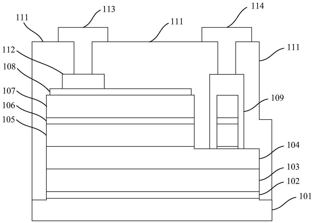
[0061] Such as figure 2 As shown, this embodiment provides an LED chip, and the LED chip is used in an LED display module. The basic structure of the LED chip is as in Embodiment 1, wherein the difference from Embodiment 1 is that the first electrode Including a first bottom electrode 110 and a first outer electrode 113, the second electrode includes a second bottom electrode 109 and a second outer electrode 114, and the anti-reflection layer 112 is used as the first bottom electrode 110 to connect the The ITO transparent conductive layer 108 and the first outer electrode 113 . In this embodiment, the anti-reflection layer 112 is used as the first bottom electrode 110, which can effectively save process steps and reduce process costs.

Embodiment 3

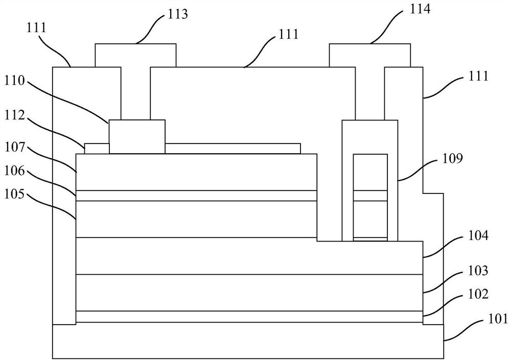
[0063] Such as image 3 As shown, this embodiment provides an LED chip, and the LED chip is used in an LED display module. The basic structure of the LED chip is as in Embodiment 1, wherein the difference from Embodiment 1 is that the anti-reflection layer 112 includes a low-reflectivity conductive material, and the anti-reflection layer 112 forms an ohmic contact with the P-type semiconductor layer 107 to simultaneously serve as a current spreading layer, and the first electrode communicates with the P-type semiconductor layer 107 through the anti-reflection layer 112 The semiconductor layer 107 is electrically connected. The LED chip of this embodiment does not need to make an additional ITO transparent conductive layer 108, and the anti-reflection layer 112 directly forms an ohmic contact with the P-type semiconductor layer 107, which not only plays the role of current diffusion, but also plays the role of reducing light reflection, which can effectively simplify the proces...


PUM

PropertyMeasurementUnit
thicknessaaaaaaaaaa
thicknessaaaaaaaaaa
thicknessaaaaaaaaaa

Abstract

The invention provides an LED chip, a display screen module and a display screen. The LED chip comprises an N-type semiconductor; a light-emitting layer which is located above the N-type semiconductor layer; a P-type semiconductor layer which is positioned above the light-emitting layer; an anti-reflection layer which covers the P-type semiconductor layer and is used for absorbing light rays which are emitted from the light-emitting layer and finally emitted to the anti-reflection layer; and a first electrode and a second electrode which are located above the P-type semiconductor layer and the N-type semiconductor layer respectively and electrically connected with the P-type semiconductor layer and the N-type semiconductor layer respectively. According to the invention, the reflection of light from the back of the LED chip can be effectively reduced, so that the light emission is reduced, the brightness of the LED chip is reduced, and the LED chip can work in a linear region without the problem of overhigh brightness; meanwhile, the thickness of the black film layer applied to the LED display screen module can be reduced, so that the display screen module has better ink color consistency.

Description

technical field [0001] The invention belongs to the field of design and manufacture of semiconductor displays, in particular to an LED chip, a display module and a display. Background technique [0002] In the application of LED chips, the application of ordinary LED chips is mainly in lighting and display backlight modules, while the current rapid development of Mini LED is mainly used in indoor and outdoor display screens. [0003] In the current LED chip, most of its design is based on lighting applications, such as the use of patterned substrates, distributed Bragg reflection layers, etc., and the currently used Mini LED also uses the same design. This type of chip does not have any problems in the field of lighting or backlight, but it has a major defect in the field of display: excessive brightness affects the comfort of the display. In order to make the luminance of the LED chip more suitable, the existing solution is to drive the LED chip with a small current. When...

Claims


Application Information

Patent Timeline
Patent Type & Authority Applications(China)
IPC IPC(8): H01L33/44H01L33/14H01L25/075H01L27/15G09F9/33G02B5/00
CPCH01L33/44H01L33/14H01L25/0753H01L27/156G09F9/33G02B5/003
Inventor 刘权锋胡现芝付小朝庄文荣孙明卢敬权
Owner 东莞市中晶半导体科技有限公司
Why Eureka
Try Eureka