Small-pitch display module and manufacturing method thereof
A technology for a display module and a manufacturing method, which is applied in semiconductor/solid-state device manufacturing, semiconductor/solid-state device components, semiconductor devices, etc., can solve problems such as open circuit and LED chip damage, and achieve broad application prospects and low production costs. , to avoid the effect of LED chip damage or open circuit
- Summary
- Abstract
- Description
- Claims
- Application Information
AI Technical Summary
Problems solved by technology
Method used
Image

Examples
Embodiment 1
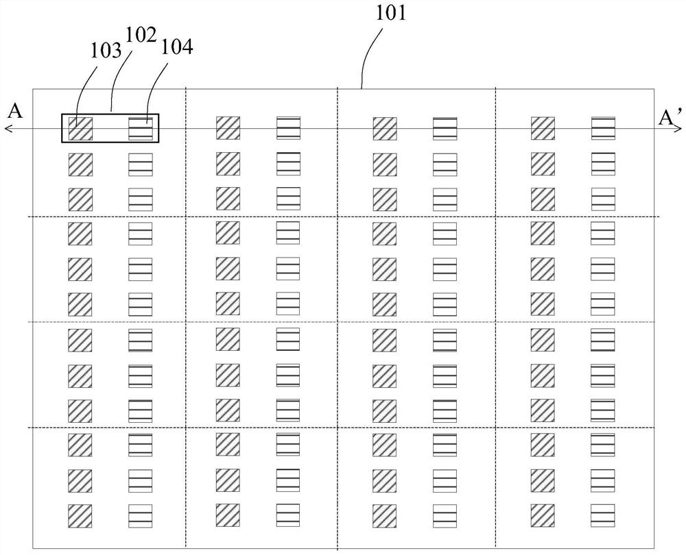
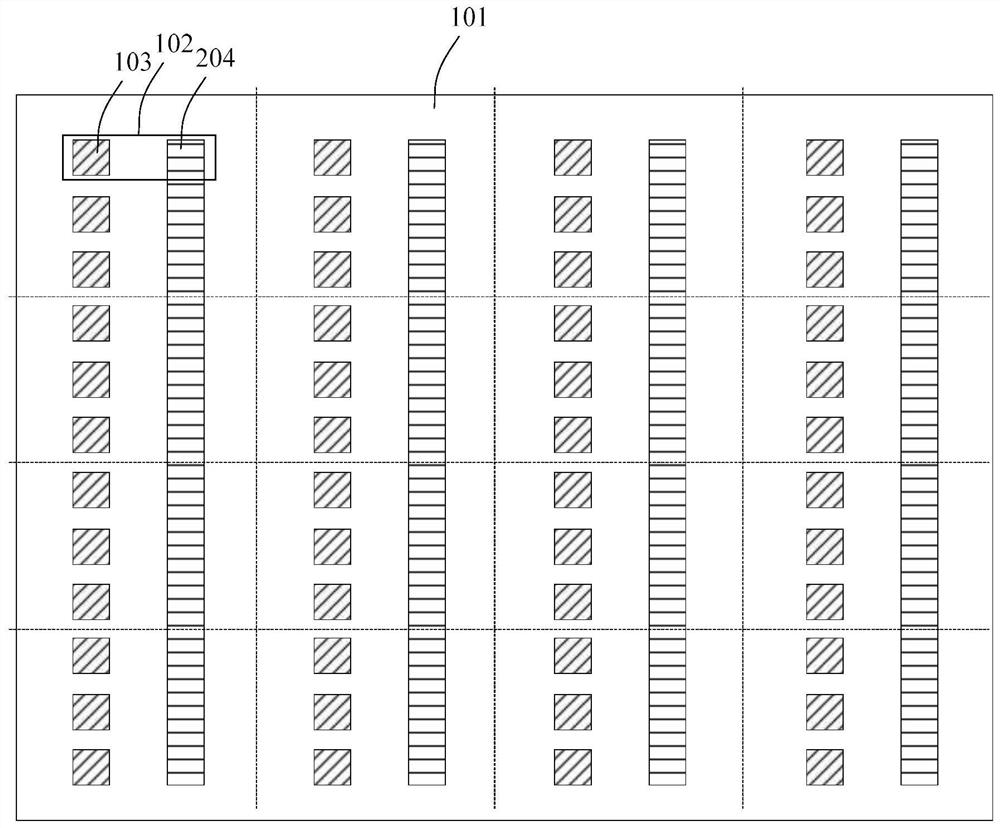
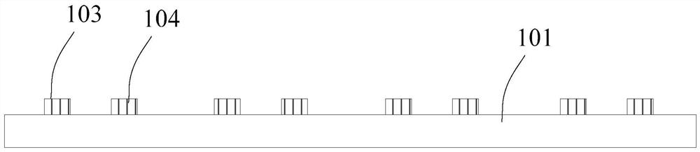
[0052] Such as Figure 1a ~ Figure 3b and Image 6 As shown, this embodiment provides a small-pitch display module. The small-pitch display module includes a PCB substrate 101 , a Mini LED chip 102 , a filling layer 107 and an encapsulation layer 110 .
[0053] Such as Figure 1a and figure 2 As shown, among them, figure 2 shown as Figure 1a The schematic diagram of the cross-sectional structure at AA' in the middle, the PCB substrate 101 includes a first surface and a second surface, the first surface has electrodes for connecting with the Mini LED chip 102, and the second surface has a connecting part , used to connect with the driver chip. There are interconnecting wires inside the PCB substrate 101, which can be a single-layer or multi-layer board, and the electrodes include a first electrode 103 and a second electrode 104, and the first electrode 103 and the second electrode 104 are point electrodes. electrode, the first electrode 103 can be positive or negative, ...
Embodiment 2
[0093] Such as Figure 11 ~ Figure 13 As shown, this embodiment provides a small-pitch display module, the basic structure of which is the same as that of Embodiment 1, wherein the difference from Embodiment 1 lies in: the top of the Mini LED chip 102 and the encapsulation layer 110 There is also a window layer 109 between them, and the top surface of the filling layer 107 may be higher than the top surface of the Mini LED chip 102 and lower than the top surface of the window layer 109 . The material of the window layer 109 includes transparent resin, and the resin includes one of silicone resin and epoxy resin. The window layer 109 partially covers the Mini LED chip, and the shape of the window layer 109 includes one or more combinations of rectangle, triangle, pentagon, trapezoid, circle and ellipse. Corresponding to different Mini LED chips 102, the window layer 109 can be designed in different shapes or sizes, for example, as Figure 12 As shown, the window layer 109 can...
PUM
 Abstract
Description
Claims
Application Information