Chip packaging structure and chip packaging method

A technology of chip packaging structure and packaging structure, which is applied in the direction of sustainable manufacturing/processing, climate sustainability, semiconductor devices, etc., can solve the problems of single function and inability to realize bidirectional sensing of image sensors, etc., so as to reduce maintenance costs and shrink The effect of device assembly size

Active Publication Date: 2020-09-29
FOREHOPE ELECTRONICS NINGBO CO LTD
View PDF3 Cites 0 Cited by
  • Summary
  • Abstract
  • Description
  • Claims
  • Application Information

AI Technical Summary

Problems solved by technology

[0003] The packaging structure of the traditional image sensor chip can only be used for photosensitive on one side, and cannot realize bidirectional sensing of the image sensor, and the function is relatively single

Method used


Image

  • Chip packaging structure and chip packaging method
  • Chip packaging structure and chip packaging method
  • Chip packaging structure and chip packaging method

Examples


Embodiment Construction

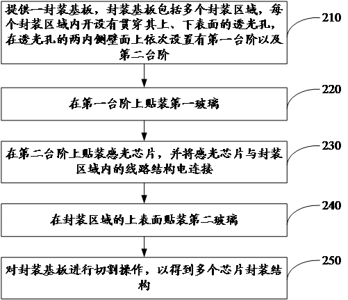
[0049] The technical solutions in the embodiments of the present application will be described below with reference to the drawings in the embodiments of the present application.

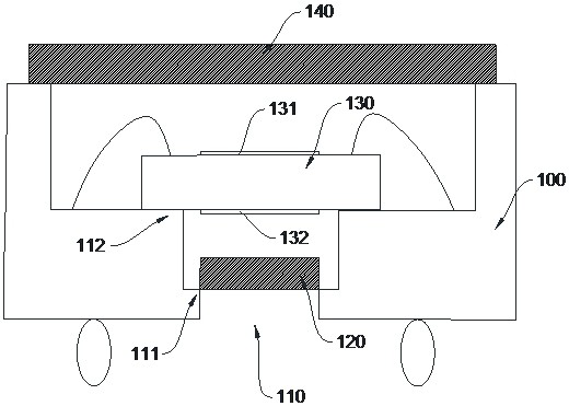
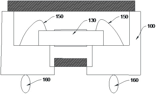
[0050] An embodiment of the present application provides a chip packaging structure, which can realize double-sided imaging of an image sensor. Figure 1~Figure 2 shows a side view of the chip package structure, as Figure 1~Figure 2 As shown, the chip package structure includes:

[0051] A substrate 100, on which there are light-transmitting holes 110 penetrating through its upper and lower surfaces, and a first step 111 and a second step 112 are sequentially arranged on both inner sidewalls of the light-transmitting hole 110;

[0052] The two first steps on the two inner wall surfaces are opposite to each other, and the two second steps on the two inner wall surfaces are opposite to each other.

[0053] A first glass 120, which is arranged on the first step 111;

[0054] A photosensitive chip 130...


PUM

PropertyMeasurementUnit
transmittivityaaaaaaaaaa

Abstract

The present application provides a chip packaging structure and a chip packaging method, which relate to the technical field of chip packaging. Specifically, the present application sets a light-transmitting glass at the upper and lower ends of the substrate, so that light can reach the photosensitive area on the upper surface of the photosensitive chip from the light-transmitting glass on the top of the substrate, thereby realizing the light sensing function on the top of the substrate. The light-transmitting glass at the bottom of the substrate reaches the photosensitive area on the lower surface of the photosensitive chip to realize the light sensing function at the bottom of the substrate. Therefore, the obtained chip packaging structure can realize double-sided sensing and imaging of the photosensitive chip, which is conducive to having more integrated image processing functions. When applied to image processing equipment, the assembly size of the equipment can be greatly reduced.

Description

technical field [0001] The present application relates to the technical field of chip packaging, and in particular, to a chip packaging structure and a chip packaging method. Background technique [0002] The package of the chip plays the role of placing, fixing, sealing, protecting the chip and enhancing the electrothermal performance, and also serves as a bridge between the internal world of the chip and the external circuit. The packaging structure of the traditional image sensor chip is mainly to place the image sensor chip on the substrate, connect the chip to the substrate by wire bonding, and then paste the light-transmitting glass on top of the chip by dispensing to achieve the purpose of light transmission. Then, the stacked chips and the substrate are protected by plastic sealing, and the packaging of the image sensing chip is completed. [0003] The packaging structure of the traditional image sensor chip can only be used for photosensitive on one side, and canno...

Claims


Application Information

Patent Timeline
Patent Type & Authority Patents(China)
IPC IPC(8): H01L31/0203H01L31/02H01L31/18
CPCH01L31/02005H01L31/0203H01L31/18Y02P70/50
Inventor 徐玉鹏李利钟磊
Owner FOREHOPE ELECTRONICS NINGBO CO LTD
Why Eureka
Try Eureka