Novel distributed array and cmos architecture for 2-stack 3D phase-change memory with higher array efficiency
A memory and array technology, applied in the field of three-dimensional electronic memory, can solve problems such as high cost
- Summary
- Abstract
- Description
- Claims
- Application Information
AI Technical Summary
Problems solved by technology
Method used
Image
Examples
Embodiment Construction
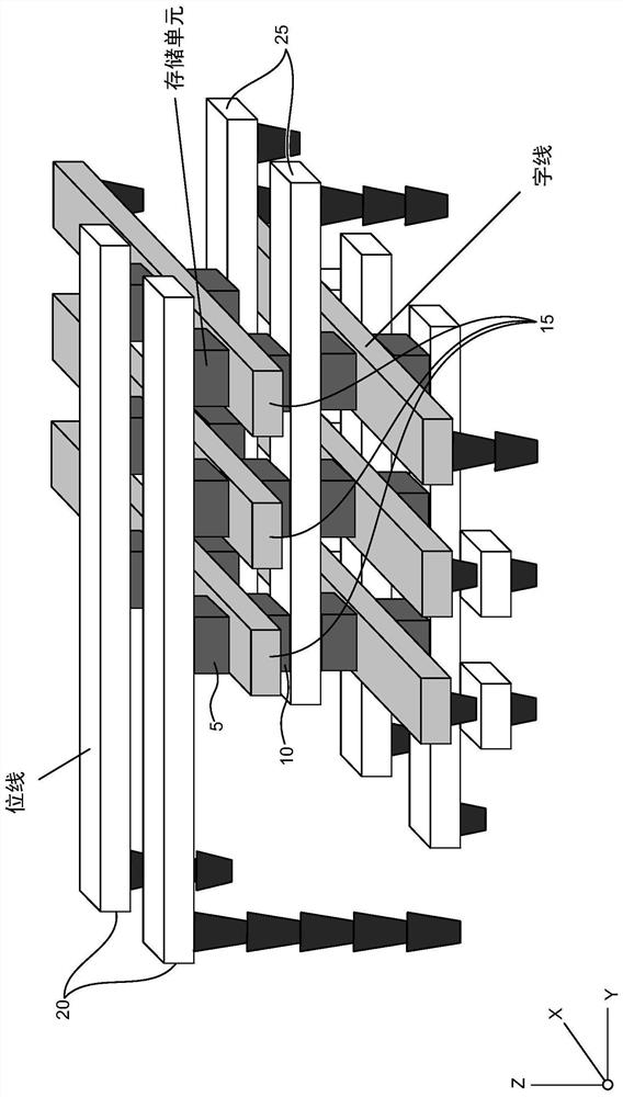
[0018] The technology is applied in the field of three-dimensional memory. exist figure 1 A general example of a three-dimensional (3D) memory is shown in . in particular, figure 1 is an isometric view of a section of a 3D phase change memory. The memory includes a first layer storage unit 5 and a second layer storage unit 10 . Between the first layer memory cells 5 and the second layer memory cells 10 are a plurality of word lines 15 extending in the horizontal (X) direction. In the depth (Z) direction, a plurality of first bit lines 20 extending along the vertical (Y) direction are above the first layer of memory cells 5, and a plurality of first bit lines 20 extending along the Y direction are below the second layer of memory cells 10. A second bit line 25.
[0019] further as figure 1 As shown in , the sequential structure of bit line, memory cell, word line, memory cell can be repeated along the Z direction to form a stacked configuration. exist figure 1 In an exa...
PUM
 Abstract
Description
Claims
Application Information


