
Compact three-dimensional memory

A technology of memory and storage devices, applied in static memory, instruments, electric solid state devices, etc., can solve problems such as difficult wiring of substrate circuits

Inactive Publication Date: 2016-09-07
HANGZHOU HAICUN INFORMATION TECH
View PDF2 Cites 1 Cited by
  • Summary
  • Abstract
  • Description
  • Claims
  • Application Information

AI Technical Summary

Problems solved by technology

However, the routing of substrate circuits becomes very difficult due to the dense via holes cutting the substrate into multiple isolated regions

Method used


Image

  • Compact three-dimensional memory
  • Compact three-dimensional memory
  • Compact three-dimensional memory

Examples


Embodiment Construction

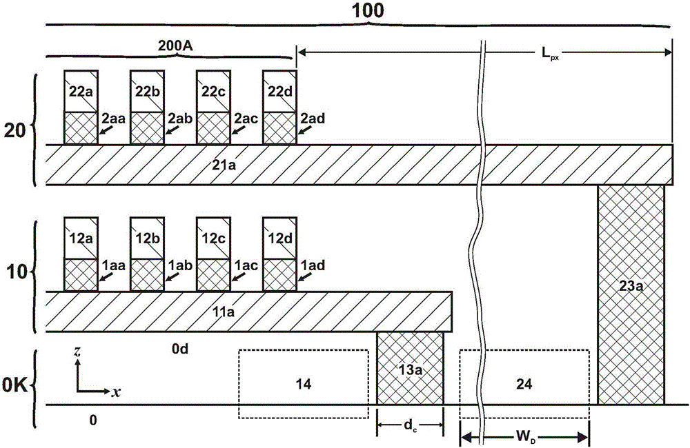
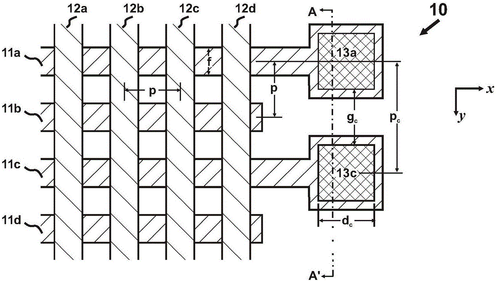
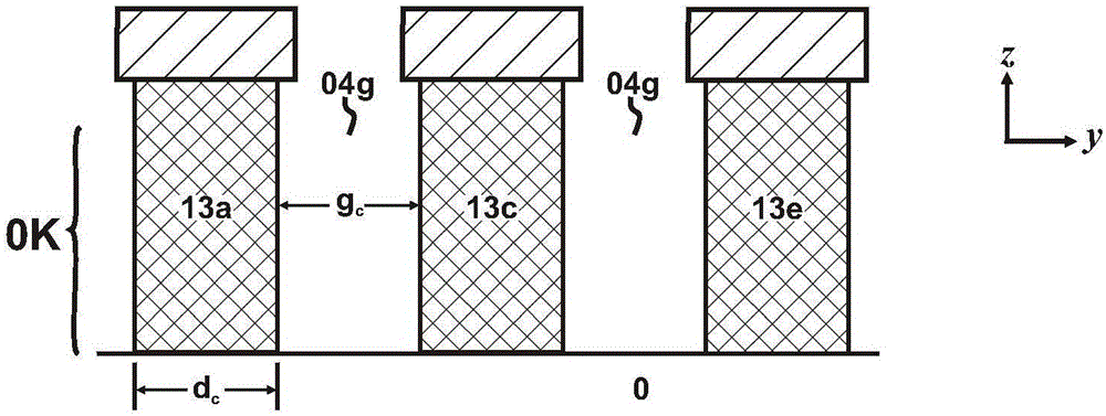
[0040] Figure 2A-Figure 2E described the first compact three-dimensional memory (3D-M C ), which includes an inner decoding stage. The 3D-M C Contains two storage layers 10, 20 stacked on the substrate 0 ( Figure 2C ). The storage layer 10 contains a storage array 100A and an intra-layer decoding stage 100P (see Figure 2A The circuit diagram in and Figure 2D top view of the ). Memory array 100A contains a plurality of x address lines 11a-11h, a plurality of y address lines 12a-12d, and a plurality of memory devices 1aa-1ad ( Figure 2A ). The intra-layer decoding stage 100P selects one address line from the two address lines of the same storage layer. It contains two control lines 17a, 17b and a plurality of simple switching devices 3aa, 3cb, 3ea, 3gb and so on. Switching device 3aa is formed at the intersection of control line 17a and x-address line 11a, between memory devices 1aa-1ad and contact via hole 13a ( Figure 2D ). The switching device 3aa is generally ...


PUM


Abstract

The present invention discloses a compact three-dimensional memory (3D-MC). By forming simple switching devices on the address-wires, a contact channel aperture can be shared by the address-wires in a same memory level, or different memory levels. The arrangement makes the channel apertures sparser and fewer, so as to realize sparse channel apertures, which have great significance to the realization of three-dimensional integrated circuit (3D-IC).

Description

technical field [0001] The present invention relates to the field of integrated circuit memories, more precisely three-dimensional memories (3D-M). Background technique [0002] Three-dimensional memory (3D-M) is a monolithic semiconductor memory that consists of multiple memory cells (also called memory devices) stacked on top of each other. 3D-M includes three-dimensional read-only memory (3D-ROM) and three-dimensional random access memory (3D-RAM). 3D-ROM can be further divided into three-dimensional mask programmed read-only memory (3D-MPROM) and three-dimensional electrically programmed read-only memory (3D-EPROM). Based on its programming mechanism, 3D-M can contain memristor, resistive random-access memory (RRAM or ReRAM), phase-change memory (PCM), programmable metallization memory (PMM), or conductive-bridging random-access memory (CBRAM), etc. . [0003] US Patent 5,835,396 discloses a 3D-M (3D-ROM) (Fig. 1A). It contains a semiconductor substrate 0 and substra...

Claims


Application Information

Patent Timeline
IPC IPC(8): G11C5/02H01L27/10
Inventor 张国飙
Owner HANGZHOU HAICUN INFORMATION TECH
Learn More