Novel distributed array and contact architecture for 4 stacked 3D PCM memories

A memory and contact technology, applied in semiconductor devices, electric solid state devices, electrical components, etc., can solve problems such as high cost

Pending Publication Date: 2020-10-09
YANGTZE ADVANCED MEMORY INDUSTRIAL INNOVATION CENTER CO LTD
View PDF3 Cites 4 Cited by
  • Summary
  • Abstract
  • Description
  • Claims
  • Application Information

AI Technical Summary

Problems solved by technology

However, as the feature size of memory cells approaches the lower limit, planar processes and fabrication techniques become challenging and costly
Therefore, the storage density of planar memory cells approaches the upper limit

Method used


Image

  • Novel distributed array and contact architecture for 4 stacked 3D PCM memories
  • Novel distributed array and contact architecture for 4 stacked 3D PCM memories
  • Novel distributed array and contact architecture for 4 stacked 3D PCM memories

Examples


Embodiment Construction

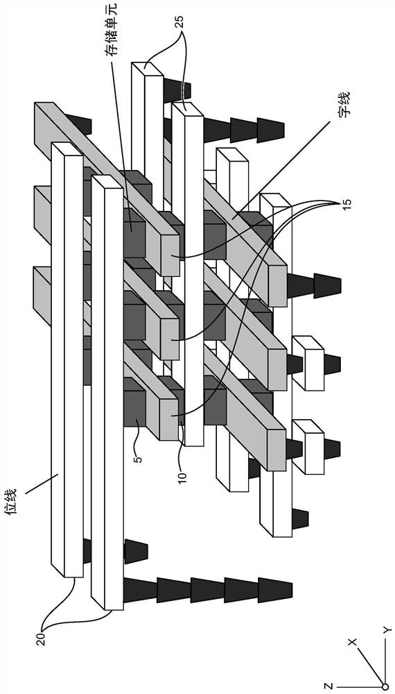
[0015] The technology is applied in the field of three-dimensional memory. exist figure 1 A general example of a three-dimensional (3D) memory is shown in . in particular, figure 1 A perspective view of a portion of a 3D phase change memory (PCM) is shown. exist figure 1 Among them, the memory includes a first layer storage unit 5 and a second layer storage unit 10 . Between the first layer memory cells 5 and the second layer memory cells 10 are a plurality of word lines 15 extending in the horizontal (X) direction. In the depth (Z) direction, a plurality of first bit lines 20 extending along the vertical (Y) direction are above the first layer of memory cells 5, and a plurality of first bit lines 20 extending along the Y direction are below the second layer of memory cells 10. A second bit line 25.

[0016] further as figure 1 As shown in , the sequential structure of bit line, memory cell, word line, memory cell can be repeated along the Z direction to form a stacked ...


PUM


Abstract

A three-dimensional memory includes memory cell layers stacked in a depth direction. The bottom cell layer includes a bottom cell array block, the top cell layer includes a top cell array block aligned with the bottom cell array block in a vertical direction, and the at least one intermediate cell layer includes an intermediate cell array block offset from the bottom cell array block in the vertical direction. The memory includes a plurality of bit lines and a plurality of bit line contacts, where a bottom cell bit line contact is connected to the bottom cell bit line, a top cell bit line contact is connected to the top cell bit line and the bottom cell bit line, and an intermediate cell bit line contact is connected to the intermediate cell bit line and located in a space between the bottom cell array blocks.

Description

technical field [0001] In general, the present disclosure relates to three-dimensional electronic memory, and in particular, the present disclosure relates to increasing the density of memory cells in three-dimensional phase change memory (3D PCM). Background technique [0002] Planar memory cells are shrunk to smaller sizes by improving process technology, circuit design, programming algorithms, and manufacturing processes. However, as the feature size of memory cells approaches the lower limit, planar processes and fabrication techniques become challenging and costly. Therefore, the storage density of planar memory cells approaches the upper limit. There remains a need for three-dimensional (3D) memory architectures that can address the density limitations in planar memory cells. Contents of the invention [0003] The three-dimensional memory and methods disclosed herein solve the problems of the state of the art and provide additional benefits. According to one aspec...

Claims


Application Information

Patent Timeline
Patent Type & Authority Applications(China)
IPC IPC(8): H01L45/00H01L27/24
CPCH10B63/84H10N70/231H10N70/011H10N70/826
Inventor 刘峻
Owner YANGTZE ADVANCED MEMORY INDUSTRIAL INNOVATION CENTER CO LTD
Why Eureka
Try Eureka