Array substrate, display panel and electronic equipment

A technology for array substrates and display panels, applied to circuits, electrical components, electrical solid-state devices, etc., can solve problems such as poor image quality

Inactive Publication Date: 2020-10-27
YUNGU GUAN TECH CO LTD
View PDF4 Cites 6 Cited by
  • Summary
  • Abstract
  • Description
  • Claims
  • Application Information

AI Technical Summary

Problems solved by technology

[0004] However, when light passes through the gap between adjacent conductive traces, i

Method used


Image

  • Array substrate, display panel and electronic equipment
  • Array substrate, display panel and electronic equipment
  • Array substrate, display panel and electronic equipment

Examples


Embodiment Construction

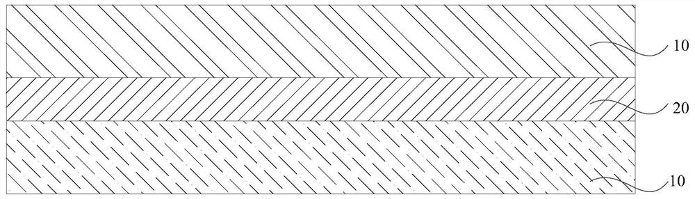
[0041] One of the main reasons for the diffraction phenomenon when light passes through the transparent display area is that the conductive traces between any adjacent film layers in the transparent display area are usually arranged in a straight line and parallel to each other. The shape of the formed gap is a regular shape such as a rectangle, and it is regularly arranged. When the light passes through the gap between adjacent conductive traces, diffraction phenomenon will occur, forming diffraction stripes or halos, resulting in the image captured by the photosensitive element The quality is poor, and even defects such as image distortion appear.

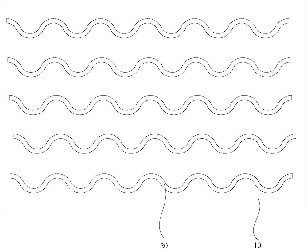
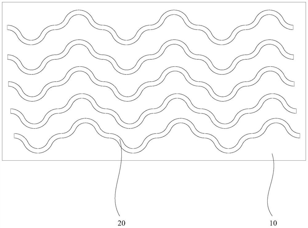
[0042] In order to solve the above problems, in the array substrate provided by the embodiment of the present invention, the shape of the conductive wires between any two adjacent film layers in the transparent display area is arranged in a preset function curve, so that the distance between the adjacent conductive wires The shap...


PUM


Abstract

The invention provides an array substrate, a display panel and electronic equipment, relates to the technical field of display, and is used for solving the technical problem that external light diffracts when penetrating through a transparent display area. The array substrate comprises a transparent display area and a non-transparent display area adjacent to the transparent display area, wherein the transparent display area comprises a plurality of film layers which are sequentially arranged in a stacked mode and conductive wires located between any two adjacent film layers, and the conductivewires are arranged in a preset function curve shape. The array substrate provided by the invention is used for improving the diffraction phenomenon generated when light penetrates through the transparent display area, so that the quality of an image acquired by a photosensitive element is improved.

Description

technical field [0001] The present invention relates to the field of display technology, in particular to an array substrate, a display panel and electronic equipment. Background technique [0002] With the rapid development of electronic equipment, full screen display has become a development trend of electronic equipment such as mobile phones. In order to realize a full-screen display, photosensitive elements such as a camera are usually arranged below the display panel to form an under-screen camera. [0003] In an electronic device using an under-screen camera, the display panel usually includes a transparent display area and a non-transparent display area surrounding the transparent display area. The photosensitive elements such as the under-screen camera correspond to the positions of the transparent display area. The multiple film layers, and the conductive lines between any adjacent film layers, the external light passes through the gap between the adjacent conducti...

Claims


Application Information

Patent Timeline
IPC IPC(8): H01L27/32G02F1/1362G09F9/33
CPCG02F1/136286G09F9/33H10K59/65H10K59/131H01L27/124H10K59/121H10K59/179
Inventor 陈昊康梦华丁立薇刘如胜
Owner YUNGU GUAN TECH CO LTD
Why Eureka
Try Eureka