Thin film solar cell and manufacturing method thereof

a solar cell and thin film technology, applied in the direction of solid-state devices, pv power plants, semiconductor devices, etc., can solve the problems of short-circuit faults, increased equipment costs as well as manufacturing cycles, and increased effect, so as to increase light diffraction, high reflective effect, and increase light transmission efficiency

Inactive Publication Date: 2013-05-21
NEXPOWER TECH
View PDF7 Cites 5 Cited by
  • Summary
  • Abstract
  • Description
  • Claims
  • Application Information

AI Technical Summary

Benefits of technology

[0006]Accordingly, a primary objective of the present invention is to provide a manufacturing method of a stacked-layered thin film solar cell, wherein the mask with the plural patterns allows the formation of the interlayer and the isolating treatment thereof in one step, thereby reducing manufacturing costs.
[0007]A secondary objective of the present invention is to provide a manufacturing method of a stacked-layered thin film solar cell, wherein the mask with the plural patterns allows the interlayer to be divided into plural said segments in one step, thereby increasing light diffraction paths and improving light transmission efficiency.
[0008]Another objective of the present invention is to provide a manufacturing method of a stacked-layered thin film solar cell, wherein the division and layout of the interlayer can be adjusted by altering the patterns on the mask, thereby reducing manufacturing costs.
[0010]Therefore, another objective of the present invention is to provide a stacked-layered thin film solar cell, wherein the interlayer is opaque and highly reflective, thereby increasing the light transmission efficiency of the stacked-layered thin film solar cell.
[0011]Yet another objective of the present invention is to provide a stacked-layered thin film solar cell, wherein by altering the patterns of the mask, the layout of the light transmissive regions on the interlayer can be modified, thereby increasing light diffraction and improving the light transmission efficiency of the stacked-layered thin film solar cell.

Problems solved by technology

Since the isolation grooves are formed by two types of laser beams of different wavelengths, the manufacturing procedures are complicated and therefore equipment costs as well as manufacturing cycle are enlarged.
Furthermore, after the cutting process is performed, due to possible unevenness of the laser beams, part of the second electrode layer may be not fully removed and, in its melt state, remains on the first electrode layer, leading to short-circuit faults.
Though using a single type of laser in length to process the three layers facilitates simplifying the manufacturing procedures, it is notable that the resultant thermal effect is greater and thus the induced short-circuit problem is more significant.
Moreover, when thermal treatment is implemented at the late stage of the manufacturing procedures to oxidize the semi-conductor layer and thereby increase its resistance for averting the short-circuit problem, equipment costs and manufacturing cycle can be accordingly increased.
Since the interlayer, for connecting materials of different energy levels, possesses electric conductivity, electric leakage and short-circuit faults can easily happen during an edge isolating process of the interlayer.
However, all of theses conventional approaches fail to address solutions to short-circuit faults at the edge of the battery.

Method used


Image

  • Thin film solar cell and manufacturing method thereof
  • Thin film solar cell and manufacturing method thereof
  • Thin film solar cell and manufacturing method thereof

Examples


Embodiment Construction

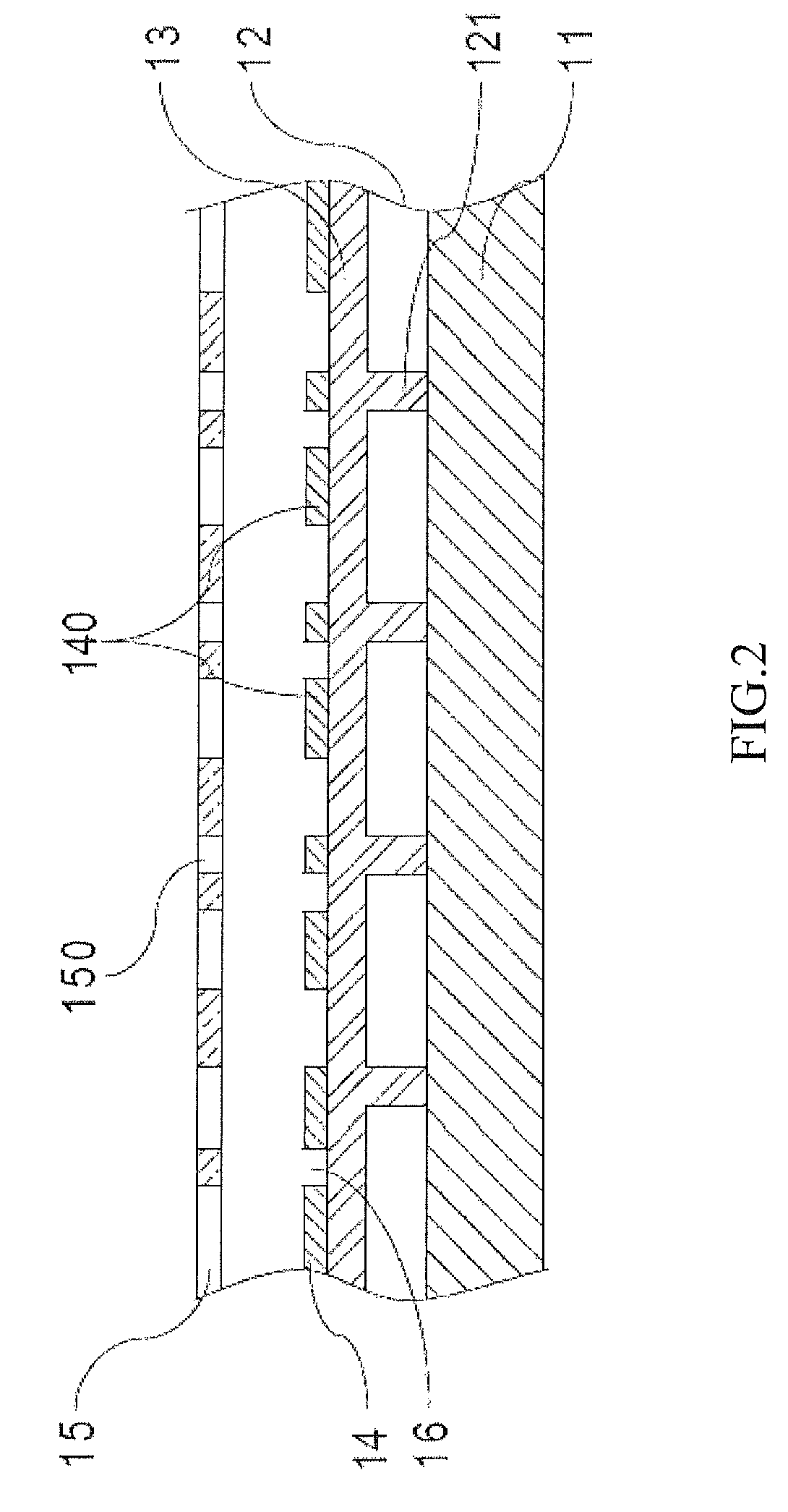
[0018]The present invention provides a stacked-layered thin film solar cell and a manufacturing method thereof, wherein the principle of photoelectric conversion of solar cells is well known to a person of ordinary skill in the art and therefore will not be detailed herein. Besides, it is to be understood that the drawings referred to in the following description are intended to demonstrate features of the present invention only schematically, so the drawings are not need to be made in scale.

[0019]The present invention herein discloses a first preferred embodiment for a stacked-layered thin film solar cell manufacturing method with the particulars discussed below.

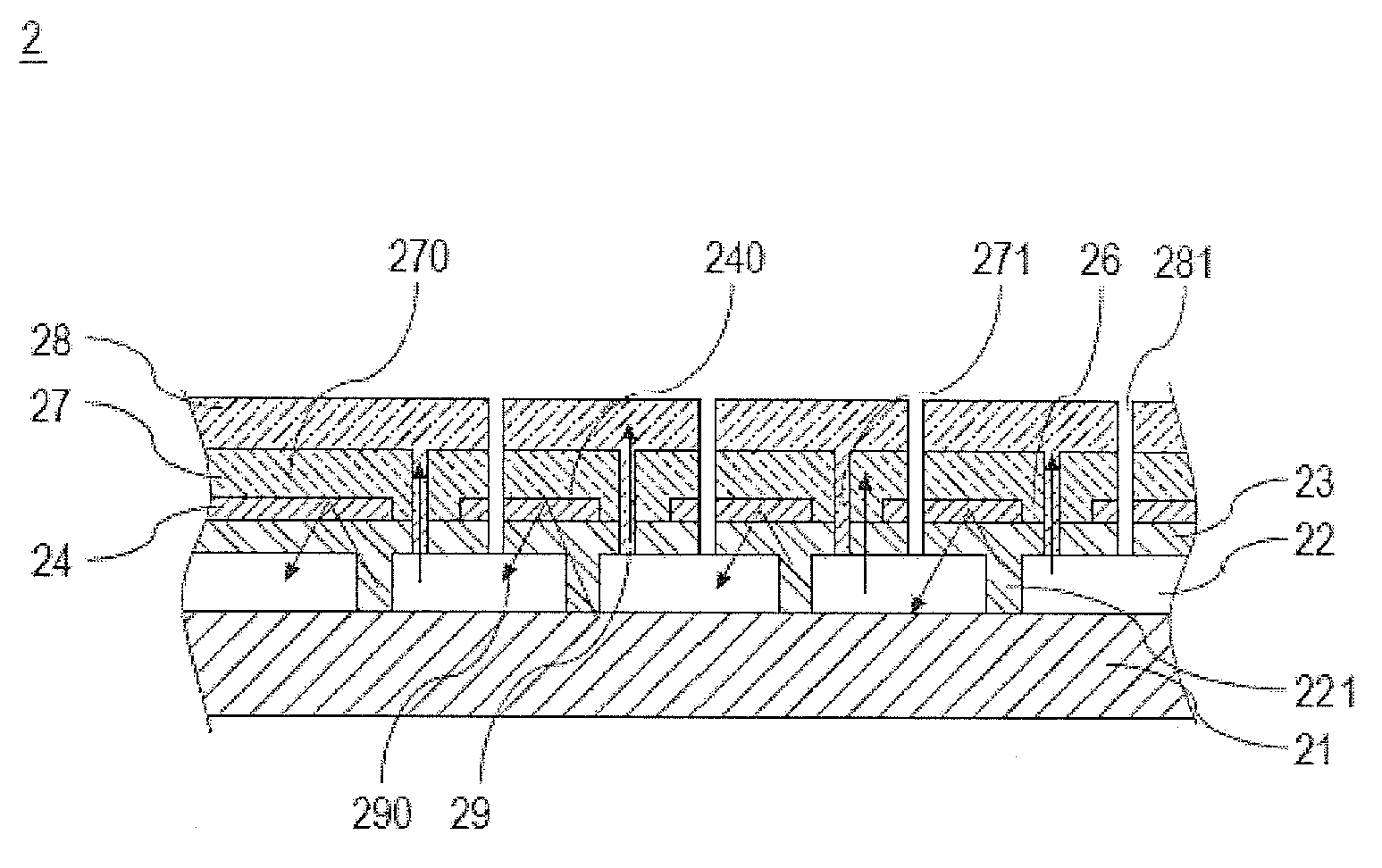
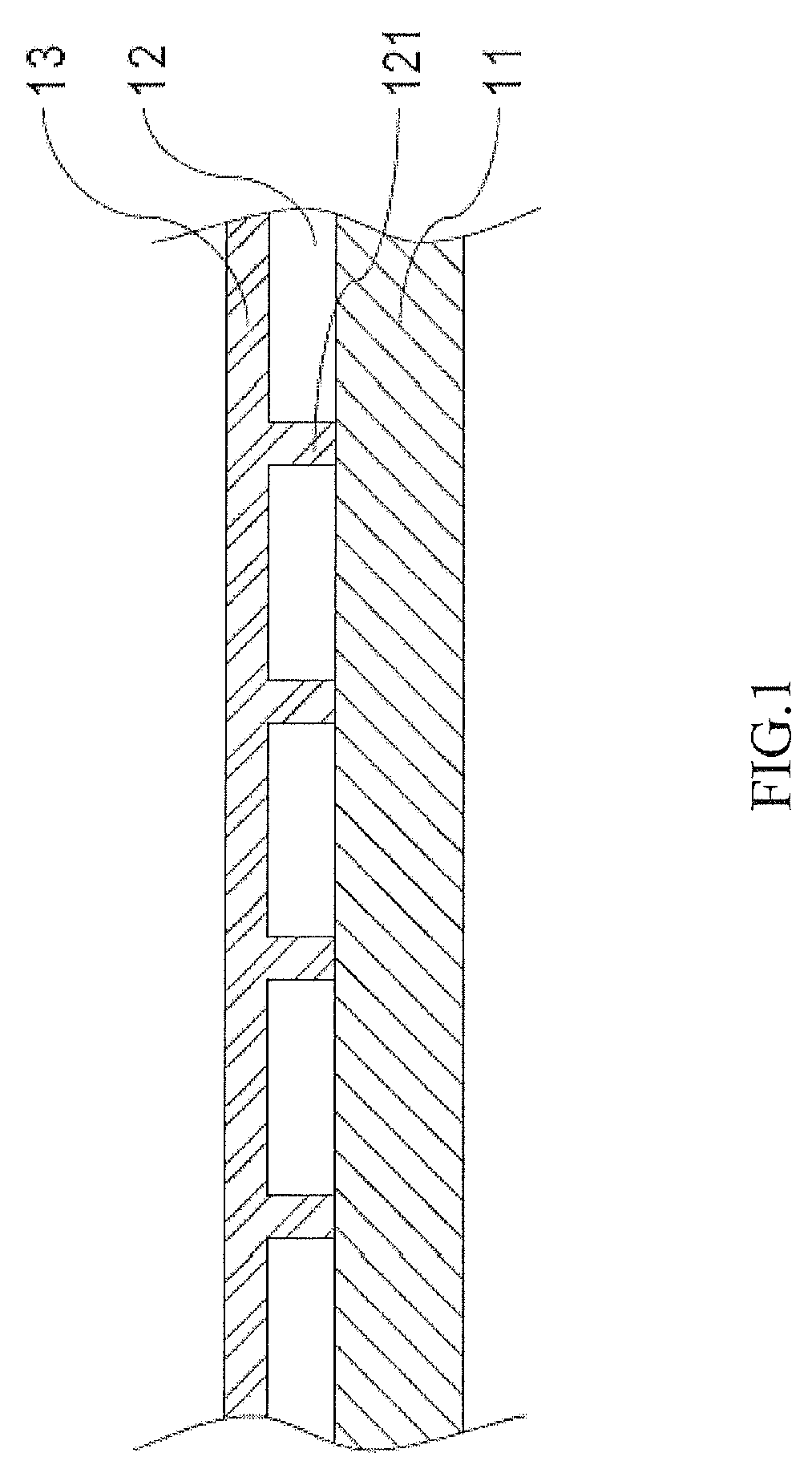
[0020]Referring to FIG. 1, firstly, a substrate 11 that is transparent is provided and formed thereon with a first electrode layer 12 by means of sputtering deposition, atmospheric pressure chemical vapor deposition or low pressure chemical vapor deposition. The material from which the first electrode layer 12 is made can b...


PUM


Abstract

The present invention provides a stacked-layered thin film solar cell and manufacturing method thereof The manufacturing method includes the steps of: providing a substrate, a first electrode layer and a first light-absorbing layer; providing a mask with a plurality of patterns above the first light-absorbing layer; forming an interlayer made of an opaque, highly reflective material by providing the mask on the first light-absorbing layer, wherein the interlayer has a plurality of light transmissive regions corresponding to the patterns, and the light transmissive regions are provided to divide the interlayer into a plurality of units; and then depositing a second light-absorbing layer on the units and a second electrode layer on the second light-absorbing layer.

Description

BACKGROUND OF THE INVENTION[0001]1. Technical Field[0002]The present invention relates to a stacked-layered thin film solar cell and a manufacturing method thereof. More particularly, the present invention relates to a manufacturing method which forms an interlayer and creates an isolation effect for a stacked-layered thin film solar cell by using a mask.[0003]2. Description of Related Art[0004]Generally speaking, a conventional stacked-layered thin film solar cell comprises a substrate, a first electrode layer, a light-absorbing layer and a second electrode layer in a series stacked structure. In a following packaging process, for eliminating problems about short-circuit faults and electric leakage, U.S. Pat. No. 6,300,556 proposes a method involving forming an isolation groove by scribing the solar cell near a periphery thereof for partially removing the first electrode layer, the semi-conductor layer and the second electrode layer, and the mechanically removing the first electrod...

Claims


Application Information

Patent Timeline
Patent Type & Authority Patents(United States)
IPC IPC(8): H01L21/00
CPCH01L31/02168H01L31/022466H01L31/056H01L31/076Y02E10/52Y02E10/548
Inventor BI, CHIEN-CHUNGLU, CHUN-HSIUNG
Owner NEXPOWER TECH
Why Eureka
Try Eureka