Diffractive optical element, design method thereof and application thereof to solar cell

a diffractive optical element and design method technology, applied in the field of optical elements, can solve the problems of difficult to be precisely controlled, limited application high manufacturing cost, and achieve the effects of enhancing the diffraction efficiency of diffractive optical elements, reducing costs, and improving flexibility in selecting modulation thickness

Active Publication Date: 2014-10-02
INST OF PHYSICS - CHINESE ACAD OF SCI
View PDF8 Cites 4 Cited by
  • Summary
  • Abstract
  • Description
  • Claims
  • Application Information

AI Technical Summary

Benefits of technology

[0037]1) The diffractive optical element and its design method according to the present invention break through limitations to the modulation thicknesses / modulation phases in the prior art so that the modulation thickness of the diffractive optical element can be selected from a larger range, thereby improving flexibility in selecting the modulation thickness of the diffractive optical element.
[0038]2) Since the modulation thickness of the diffractive optical element according to the present invention can be selected from a larger range, the thickness of the diffractive optical element can be controlled arbitrarily according to actual needs and controlled within a certain range, thereby facilitating processing a master plate by using modern photolithography technology and then using imprinting technique for mass production and thereby substantially reducing the cost.
[0039]3) Since the modulation thickness of the diffractive optical element according to the present invention can be selected from a larger range, a design modulation thickness better than the prior art can be found in an expanded selection range, thereby greatly enhancing the diffraction efficiency of the diffractive optical element. The theoretical diffraction efficiency of the diffractive optical element for performing color-separating and focusing simultaneously according to the present invention exceeds 79%.
[0040]4) Since the diffractive optical element according to the present invention greatly enhances the diffraction efficiency of the diffractive optical element, the color-separating and focusing diffractive optical element has practical application significance in solar cells. In combination with mass production through a modern lithographic technique as previously stated, this provides an efficient and low-cost way for solar energy utilization.

Problems solved by technology

Therefore, a core issue in designing the diffractive optical element is to determine a modulation thickness at each position (sampling point) of its surface.
However, the diffractive optical element designed according to the existing methods only has a diffraction efficiency of 10%-20%, thereby the diffractive optical element is limited in certain applications.
A drawback of this scheme lies in that an interface between different layers of semiconductors needs to grow by virtue of technologies such as molecular beam epitaxy, which is very difficult to be controlled precisely and has great limitation of choices of materials so as to cause the manufacture cost very high.
To achieve a higher efficiency of the color-separation, the dichroic mirror usually needs to be coated with more than ten layers or even dozes of layers of films, which is technically very difficult.
The second scheme is to use a lens-prism combination to perform color-separation, and this scheme makes the optical device bulky.
A drawback of the existing parallel configurations lies in that the cost of the optical system is very high.
However, as stated in the above description of the diffractive optical element, a diffraction efficiency of the current diffractive optical element for color-separating and focusing is only 10%-20%, such diffraction efficiency is obviously not high enough to utilization of the solar energy and hinders application of the color-separating and focusing diffractive optical element to the solar cell.

Method used


Image

  • Diffractive optical element, design method thereof and application thereof to solar cell
  • Diffractive optical element, design method thereof and application thereof to solar cell
  • Diffractive optical element, design method thereof and application thereof to solar cell

Examples


Embodiment Construction

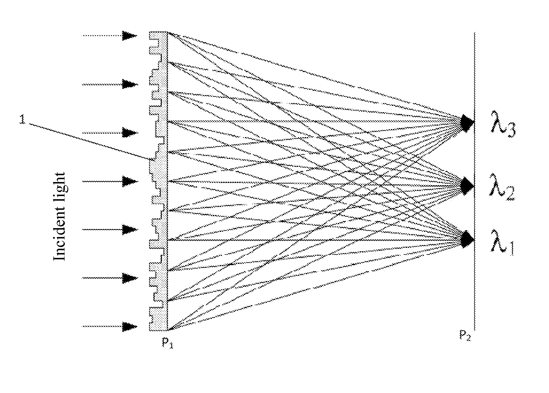
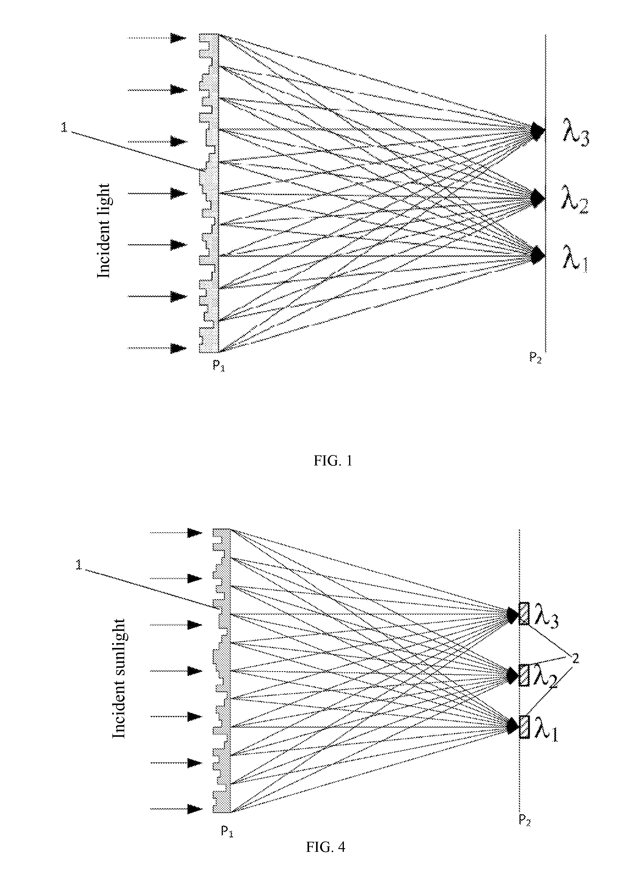
[0045]Design Ideas of a Diffractive Optical Element According to the Present Invention As shown in the illustrative optical system of FIG. 1, an incident light beam having a plurality of wavelength components λα propagates from an input plane P1 to an output plane P2 wherein α=1, 2, 3, . . . Nλ, Nλrepresents the number of different wavelengths, and Nλ is exemplarily equal to 3 in FIG. 1. The diffractive optical element 1 is adhered to the input plane P1 to modulate the phase of the incident light beam so as to obtain output light on the output plane P2, where the plurality of wavelength components are color-separated and focused. In FIG. 1, locations of λ1, λ2 and λ3 respectively represent focusing positions or areas where light wave of the corresponding wavelength components are respectively focused on the output plane P2.

[0046]Regarding the wavelength λα, its incident light wave is modulated by the diffractive optical element 1, and then has an input wave function denoted by U1α o...


PUM


Abstract

Disclosed are a diffractive optical element, a design method thereof and the application thereof in a solar cell. The design method for a design modulation thickness of a sampling point of the diffractive optical element comprises: calculating the modulation thickness of the current sampling point for each wavelength component; obtaining a series of alternative modulation thicknesses which are mutually equivalent for each modulation thickness, wherein a difference between the corresponding modulation phases is an integral multiple of 2π; and selecting one modulation thickness from the alternative modulation thicknesses of each wavelength to determine the design modulation thickness of the current sampling point. In an embodiment, the design method introduces a thickness optimization algorithm into a Yang-Gu algorithm. The design method breaks through limitations to the modulation thicknesses/modulation phases in the prior art and increases the diffraction efficiency, and the obtained diffractive optical element facilitates mass production by a modern photolithographic technique, which greatly reduces the cost. The diffractive optical element may also be applied to the solar cell, which provides an efficient and low-cost way for solar energy utilization.

Description

FIELD OF THE INVENTION[0001]The present invention relates to the field of optics, and more specifically to a diffractive optical element, a design method thereof and application thereof to solar cell.BACKGROUND OF THE INVENTION[0002]A diffractive optical element (DOE) is an optical element performing optical functions of such as focusing, color-separation (wavelength demultiplexing), refraction, reflection and imaging based on the optical diffraction principle. A typical diffractive optical element has a micro surface-relief profile which enables the phase of an incident light beam through the diffractive optical element to change (namely, phase modulation) so as to obtain a desired or designated output light distribution. A modulation amount of the phase of the incident light beam caused by the microrelief profile on the surface of the diffractive optical element is related to its thickness, that is, modulation thickness. Therefore, a core issue in designing the diffractive optical...

Claims


Application Information

Patent Timeline
Patent Type & Authority Applications(United States)
IPC IPC(8): G02B27/42G06F17/50
CPCG02B5/188Y02E10/52G06F17/50G02B27/4222H01L31/0528H01L31/0549G02B19/0042G02B27/1086G02B27/4244G02B27/0012G02B5/18G06F30/00
Inventor YANG, GUOZHENDONG, BIZHENZHANG, YANYE, JIASHENGMENG, QINGBOHUANG, QINGLIWANG, JINZE
Owner INST OF PHYSICS - CHINESE ACAD OF SCI
Why Eureka
Try Eureka