

Chuck device in wafer cleaning equipment and wafer cleaning equipment
A technology for cleaning equipment and chucks, applied in electrical components, semiconductor/solid-state device manufacturing, circuits, etc., can solve problems such as poor versatility of chuck devices, and achieve the effect of increasing usage scenarios and improving product competitiveness.
- Summary
- Abstract
- Description
- Claims
- Application Information
AI Technical Summary
Problems solved by technology
Method used
Image

Examples
Embodiment Construction
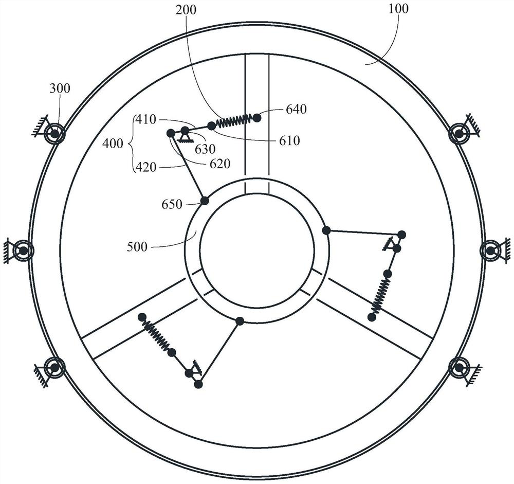
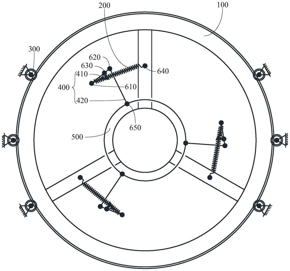
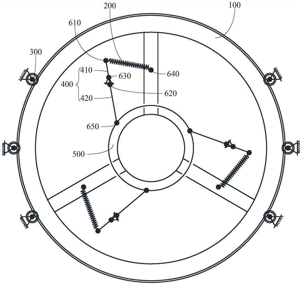
[0019] In order to make the purpose, technical solution and advantages of the present application clearer, the technical solution of the present application will be clearly and completely described below in conjunction with specific embodiments of the present application and corresponding drawings. Apparently, the described embodiments are only some of the embodiments of this application, not all of them. Based on the embodiments in this application, all other embodiments obtained by persons of ordinary skill in the art without making creative efforts belong to the scope of protection of this application.
[0020] The terms "first", "second" and the like in the specification and claims of the present application are used to distinguish similar objects, and are not used to describe a specific sequence or sequence. It is to be understood that the data so used are interchangeable under appropriate circumstances such that the embodiments of the application can be practiced in sequ...
PUM
 Abstract
Description
Claims
Application Information