An image sensor chip testing and sorting all-in-one machine

An image sensor and chip testing technology, which is applied in semiconductor/solid-state device testing/measurement, semiconductor/solid-state device manufacturing, radiation control devices, etc., can solve problems such as not being integrated in one machine, increasing the risk of chip damage or contamination, etc. , to reduce the risk of pollution, avoid elongation, and improve efficiency

Active Publication Date: 2021-06-18
技感半导体设备(南通)有限公司
View PDF5 Cites 0 Cited by
  • Summary
  • Abstract
  • Description
  • Claims
  • Application Information

AI Technical Summary

Problems solved by technology

[0003] However, there is no fusion of the three functions of high temperature, testing, and visual inspection of defects in one machine
Therefore, after the functional test is completed, it needs to be placed on a separate visual inspection machine for another inspection and screening. Such re-handling, loading and unloading, and inspection pick-and-place actions increase the risk of chip damage or contamination

Method used


Image

  • An image sensor chip testing and sorting all-in-one machine
  • An image sensor chip testing and sorting all-in-one machine
  • An image sensor chip testing and sorting all-in-one machine

Examples


Embodiment Construction

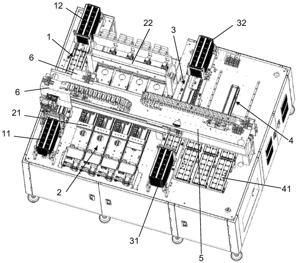
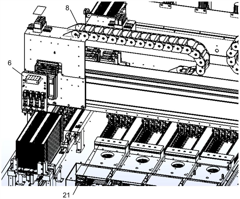
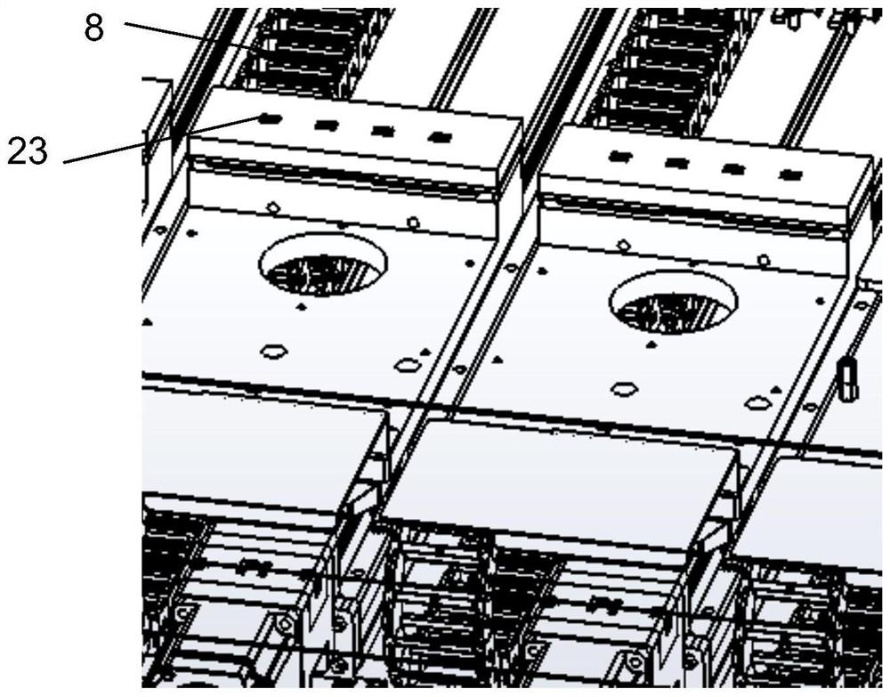
[0032] The image sensor chip testing and sorting all-in-one machine of the present invention is as follows: Figure 1-Figure 4 As shown, it mainly includes a test flow channel 1, a test flow channel 2, a good product flow channel 3, and a defective product flow channel 4, which are arranged horizontally in sequence and each has a conveying mechanism. Among them, please combine Figure 8 As shown, the conveying mechanisms in the flow channel 1 to be tested and the good product flow channel 3 all include a track 13 and a shuttle mechanism 9 arranged in the track 13, and the shuttle mechanism 9 includes a shuttle car 91 and a mechanism for driving the shuttle car 91 back and forth. The linear module 8 clamps the carrier pallet 10 through the shuttle car 91, drives the shuttle car 91 through the linear module 8 and drags the pallet 10 for backward transport, and returns empty-loaded. The front end of the flow channel 1 to be tested is provided with a tray loading bin 11 full of m...


PUM


Abstract

The invention discloses an integrated machine for testing and sorting image sensor chips. There is an empty tray unloading bin at the back end for testing full pallets; a good product full pallet unloading bin is installed at the front end of the flow channel for good products, and an empty tray loading bin is installed at the rear end; the conveying mechanism of the test flow channel is equipped with a heating function The lower test seat of the test flow channel is equipped with a matching downward pressure test mechanism; the conveying mechanism of the defective product flow channel is provided with a tray for storing defective products; there is a beam across the top of each flow channel, and the front and rear sides of the beam are A chip suction mechanism capable of moving along the beam is separately provided. Integrate multiple functions such as chip testing, heating and visual inspection into the whole sorting machine, only need to add one step of pause and photo inspection to the original action logic, which can effectively avoid the risk of damage or contamination caused by chip transfer .

Description

technical field [0001] The invention belongs to chip testing and packaging technology, in particular to an image sensor chip testing and sorting integrated machine. Background technique [0002] In the chip testing and packaging process of semiconductors, there is a type of image sensor chip that requires high-temperature heating while performing functional testing, as well as inspection of appearance defects on the tin spherical surface of the product, and is classified according to the final test and inspection results. [0003] However, there is no fusion of the three functions of high temperature, testing, and visual inspection of defects in one machine. Therefore, after the functional test is completed, it needs to be placed on a separate visual inspection machine for another inspection and screening. Such re-handling, loading and unloading, and inspection pick-and-place actions increase the risk of chip damage or contamination. Contents of the invention [0004] The...

Claims


Application Information

Patent Timeline
Patent Type & Authority Patents(China)
IPC IPC(8): H01L21/67H01L21/66H01L27/146
CPCH01L21/67103H01L21/67253H01L21/67271H01L22/20H01L27/146
Inventor 梁猛赵凯卢升林海涛
Owner 技感半导体设备(南通)有限公司
Why Eureka
Try Eureka