OLED display panel, display device and display panel preparation method

A display panel and substrate technology, which is applied in the manufacture of semiconductor/solid-state devices, electrical components, diodes, etc., can solve the problems of declining user acceptance, different sizes, and blueness at large viewing angles, and achieve the effect of improving the phenomenon of color shift

Active Publication Date: 2020-11-20
BOE TECH GRP CO LTD +1
View PDF8 Cites 3 Cited by
  • Summary
  • Abstract
  • Description
  • Claims
  • Application Information

AI Technical Summary

Problems solved by technology

[0003] For the consideration of reducing the reflectivity, the opening of the CF layer is often not very large, and generally matches the opening of the RGB pixel, which leads to the different sizes of the opening of the CF layer, so at a large viewing angle, the RGB light will appear different decays, resulting in color casts
Taking the GGRB pixel arrangement as an example, in the vertical direction, the opening size of the CF layer is relatively large, and the difference is not too large. The brightness attenuation is slow under large viewing angles, and color shift is not easy to occur; but in the horizontal direction, the opening size of the CF layer is smaller. Small, and the opening of the red CF layer
The current technology solves this color shift problem by increasing the opening size of the red color film, but after increasing the opening size of the red color film, the reflectivity will increase significantly, reducing the overall performance of the product, and the user acceptance will decline

Method used


Image

  • OLED display panel, display device and display panel preparation method
  • OLED display panel, display device and display panel preparation method
  • OLED display panel, display device and display panel preparation method

Examples


Embodiment Construction

[0029] The application will be further described in detail below in conjunction with the accompanying drawings and embodiments. It should be understood that the specific embodiments described here are only used to explain related inventions, rather than to limit the invention. It should also be noted that, for ease of description, only parts related to the invention are shown in the drawings.

[0030] It should be noted that, in the case of no conflict, the embodiments in the present application and the features in the embodiments can be combined with each other. The present application will be described in detail below with reference to the accompanying drawings and embodiments.

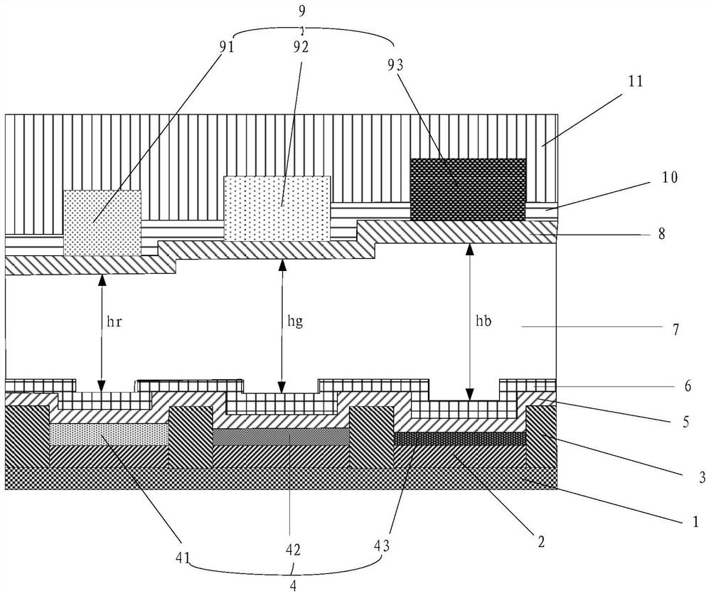
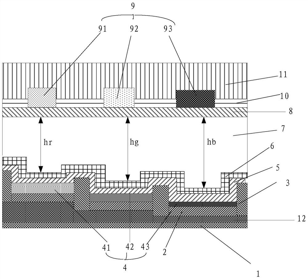
[0031] Please refer to figure 1 and figure 2 , the present embodiment provides an OLED display panel, including a luminous layer 4, the luminous layer 4 includes a plurality of sub-pixels of different colors, an organic film layer 3 is arranged between adjacent sub-pixels, and the luminous layer...


PUM

PropertyMeasurementUnit
thicknessaaaaaaaaaa

Abstract

The invention discloses an OLED display panel, a display device and a display panel preparation method, the OLED display panel comprises a light-emitting layer, the light-emitting layer comprises a plurality of sub-pixels of different colors, a color film layer is arranged above the light-emitting layer, the color film layer comprises a plurality of color films of different colors, and the light-emitting layer and the color film layer are arranged in a one-to-one correspondence manner; the opening values of the color films with different colors on the color film layer are d, the distance between each color film and the sub-pixel is L, and L is increased along with the increase of the opening value d of the color film. The opening sizes of the color films with different colors are different; the distances between the sub-pixels with different colors and the color films with the corresponding colors are changed; the visual angles of the sub-pixels of each color are the same; the color cast phenomenon of the display panel caused by too large brightness attenuation difference of the sub-pixels of different colors is further improved, the color cast phenomenon of the display panel is improved by changing the thickness of the corresponding layer structure, and other optical properties of the display panel cannot be reduced.

Description

technical field [0001] The present invention generally relates to the field of display technology, and in particular to an OLED display panel, a display device and a method for preparing the display panel. Background technique [0002] In order to prevent the reflection of the screen, the traditional OLED device needs to paste a layer of polarizer on the OLED device. The polarizer adopts the principle of polarized light, which can effectively reduce the reflection intensity of the external ambient light on the screen, but the transmittance of the polarizer Only about 44%, in order to achieve higher brightness, it is necessary to provide more power consumption. COE (Color film on EN, the color film set on the encapsulation layer) is a new technology that hopes to replace the polarizer. Its structure is to sequentially make a BM layer (light-shielding layer) on the encapsulation layer through exposure, development and other processes. , CF layer (color filter layer) and OC la...

Claims


Application Information

Patent Timeline
Patent Type & Authority Applications(China)
IPC IPC(8): H01L27/32H01L51/52H01L51/56
CPCH10K59/38H10K59/121H10K50/86H10K71/00
Inventor 黄灿李振高洪成鲍建东史大为赖韦霖杨璐王文涛
Owner BOE TECH GRP CO LTD
Why Eureka
Try Eureka