Process chambers and semiconductor processing equipment
A process chamber and chamber technology, applied in semiconductor/solid-state device manufacturing, discharge tubes, electrical components, etc., can solve problems such as increasing equipment cost and structural complexity, affecting process uniformity and production capacity, and affecting the service life of parts , to achieve the effect of improving temperature control efficiency and temperature control uniformity, improving process uniformity, and increasing production capacity
- Summary
- Abstract
- Description
- Claims
- Application Information
AI Technical Summary
Problems solved by technology
Method used
Image

Examples
no. 1 example
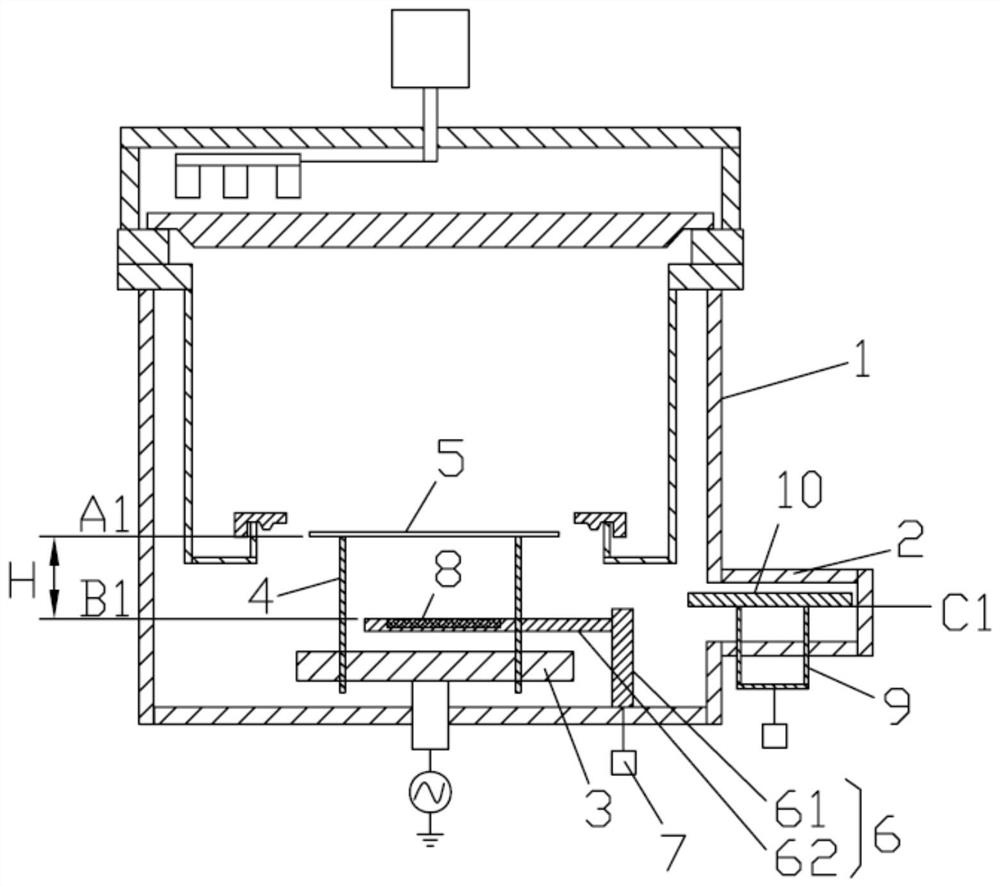
[0035] Please also refer to Figure 1A and Figure 1B , the process chamber provided in this embodiment, which can be applied to a deposition chamber, specifically includes a chamber body 1, a shielding disk library 2 communicating with the interior of the chamber body 1, a shielding disk 10 and a transmission mechanism, wherein, in The cavity main body 1 is provided with a base 3 and a first thimble mechanism 4; the base 3 is used to carry the workpiece 5 to be processed during the thin film deposition process; the first thimble mechanism 4 realizes the transfer with the base 3 by lifting Workpiece 5 to be processed. Specifically, the first thimble mechanism 4 includes at least three thimbles arranged at intervals around the axis of the base 3 and a lifting mechanism connected thereto. Driven by the lifting mechanism, the at least three thimbles can rise synchronously to a point higher than the base. The highest position of 3 or the top is lower than the lowest position of b...
no. 2 example
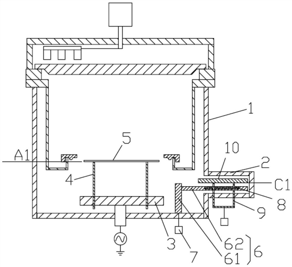
[0051] see Figure 4A , the present embodiment provides a process chamber, which, compared with the above-mentioned first embodiment, also includes a chamber main body 1 , a shadow disk library 2 , a shadow disk 10 and a transmission mechanism. Since the structures and functions of these components are the same as those of the above-mentioned first embodiment, they will not be repeated here, and only the differences between this embodiment and the above-mentioned first embodiment will be described in detail below.
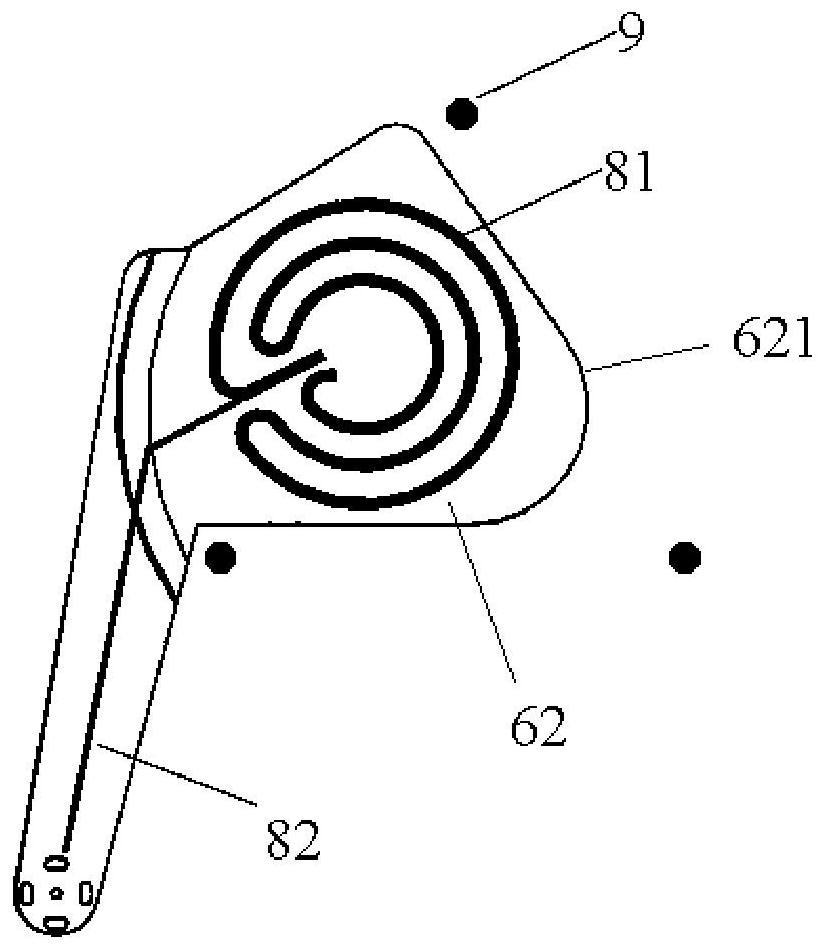
[0052] Specifically, when the transfer arm 6 is inside the chamber main body 1 , it is located above the processed workpiece carried by the first ejector mechanism 4 . Such as Figure 4A As shown, the highest position A2 of the first ejector mechanism 4 is lower than the position B2 of the transfer arm 6 inside the chamber main body 1 . In addition, the temperature control device 8 is exposed to the lower surface of the transfer arm 6 to exchange heat with the pr...
no. 3 example
[0057] see Figure 5 , the present embodiment provides a process chamber, which, compared with the above-mentioned first and second embodiments, also includes a chamber main body 1 , a shadow disk library 2 , a shadow disk 10 and a transmission mechanism. Since the structures and functions of these components are the same as those of the above-mentioned first and second embodiments, details will not be repeated here, and only the differences between this embodiment and the above-mentioned first and second embodiments will be described in detail below.
[0058] Specifically, when the transfer arm 6 moves to the interior of the chamber main body 1 and is located at a position opposite to the processed workpiece 5 carried by the first ejector mechanism 4, the processed workpiece 5 can pass through the first ejector mechanism 4 ascent or Move down to the position where it contacts with the transfer arm 6; and, the temperature control device 8' controls the temperature of the workp...
PUM
 Abstract
Description
Claims
Application Information
 - R&D
- Intellectual Property
- Life Sciences
- Materials
- Tech Scout
- Unparalleled Data Quality
- Higher Quality Content
- 60% Fewer Hallucinations
Browse by: Latest US Patents, China's latest patents, Technical Efficacy Thesaurus, Application Domain, Technology Topic, Popular Technical Reports.
© 2025 PatSnap. All rights reserved.Legal|Privacy policy|Modern Slavery Act Transparency Statement|Sitemap|About US| Contact US: help@patsnap.com