
Mask optimization method and electronic equipment

An optimization method and mask technology, applied in optics, instruments, photolithography process of pattern surface, etc., can solve problems such as the placement of evaluation points and the deviation of the moving direction of evaluation points.

Pending Publication Date: 2020-12-01
DONGFANG JINGYUAN ELECTRON LTD
View PDF0 Cites 0 Cited by
  • Summary
  • Abstract
  • Description
  • Claims
  • Application Information

AI Technical Summary

Problems solved by technology

[0004] In order to overcome the current technical problem of deviation in the position of the evaluation point and the determination of the moving direction of the evaluation point in the mask optimization process, the present invention provides a mask optimization method and electronic equipment

Method used


Image

  • Mask optimization method and electronic equipment
  • Mask optimization method and electronic equipment
  • Mask optimization method and electronic equipment

Examples


Embodiment Construction

[0035] In order to make the object, technical solution and advantages of the present invention more clear, the present invention will be further described in detail below in conjunction with the accompanying drawings and embodiments. It should be understood that the specific embodiments described here are only used to explain the present invention, not to limit the present invention.

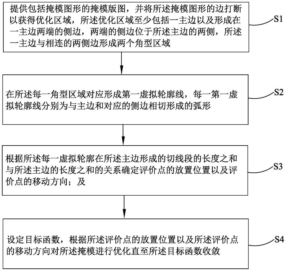
[0036] see figure 1 , the first embodiment of the present invention provides a mask optimization method, including the following steps:

[0037] S1. Provide a mask layout including a mask pattern, and break the sides of the mask pattern to obtain an optimized area, the optimized area includes at least one main side and sides formed at both ends of a main side, and the two ends The sides are located on both sides of the main side, and the one main side and the connected two sides form two angular regions;

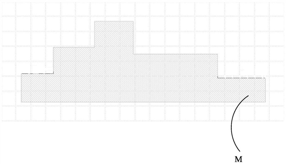
[0038] see figure 2 , in this step, the mask pattern is a long strip structure, usuall...


PUM


Abstract

The invention belongs to the field of integrated circuit mask design and relates to a mask optimization method and electronic equipment. The method comprises the following steps of: S1, breaking edgesof a mask pattern to obtain an optimized region; S2, correspondingly forming first virtual contour lines in each angular region; S3, determining the placement positions of evaluation points and the moving directions of the evaluation points according to the relationship between the sum of the lengths of tangent segments formed by each virtual contour on main edges and the sum of the lengths of the main edges; and S4, optimizing a mask until a target function converges, determining the placement positions of the evaluation points and the moving directions of the evaluation points according tothe relationship between the sum of the lengths of tangent sections formed by each virtual contour on the main edges and the sum of the lengths of the main edges. Therefore, the obtained virtual contour lines are closer to the actual contour lines of an exposure pattern, the evaluation points are placed on the virtual contour lines, the EPE in the moving directions of the determined evaluation points can well reflect the requirement for mask optimization, and a good optimization effect is achieved.

Description

【Technical field】 [0001] The invention relates to the field of integrated circuit mask design, in particular to a mask optimization method and electronic equipment. 【Background technique】 [0002] Photolithography is the core step in the manufacture of integrated circuits. Its purpose is to transfer the pattern on the mask to the photoresist coated on the silicon substrate through the optical imaging system and further transfer it to the silicon wafer. The pattern transferred to the photoresist is called the spatial image, namely AI (Aerial Image); the pattern transferred to the silicon wafer is called the resist image, namely RI (ResistImage). For the convenience of description later, these two kinds of images are collectively referred to as exposure patterns. Due to the existence of the diffraction effect of the optical imaging system, high-order diffracted light cannot participate in imaging through the lithography projection objective lens, so the exposure pattern will ...

Claims


Application Information

Patent Timeline
Patent Type & Authority Applications(China)
IPC IPC(8): G03F1/36
CPCG03F1/36
Inventor 丁明李强施伟杰
Owner DONGFANG JINGYUAN ELECTRON LTD
Learn More