Miniaturized image sensor

An image sensor and photoelectric conversion technology, which is applied in image communication, TV, color TV parts, etc., can solve the problem of small shooting range of image sensor

Pending Publication Date: 2020-12-11
WEIHAI HUALING OPTO ELECTRONICS CO LTD
View PDF0 Cites 0 Cited by
  • Summary
  • Abstract
  • Description
  • Claims
  • Application Information

AI Technical Summary

Problems solved by technology

[0004] The main purpose of the present invention is to provide a miniaturized image sensor to solve the problem that the image sensor in the prior art has a small shooting range

Method used


Image

  • Miniaturized image sensor
  • Miniaturized image sensor
  • Miniaturized image sensor

Examples


Embodiment 1

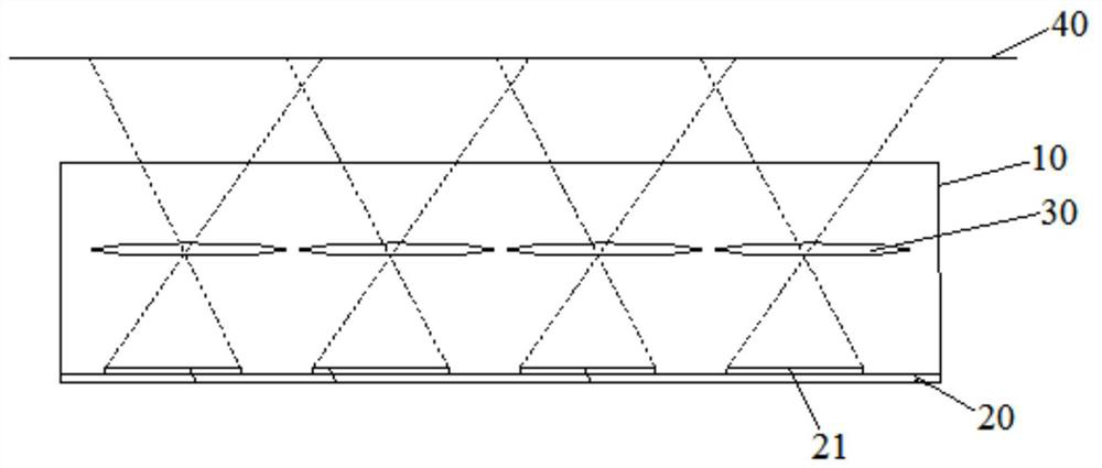
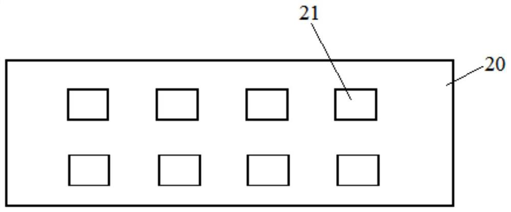
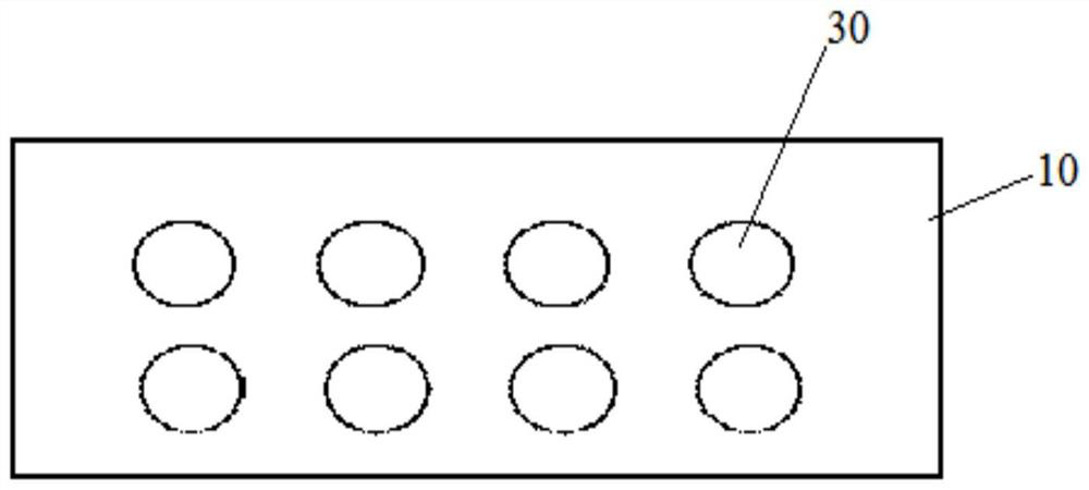
[0033] Such as Figure 1 to Figure 4 As shown, a plurality of photoelectric conversion chips 21 are arranged in a rectangular array. A plurality of photoelectric conversion chips 21 are arranged in a matrix array, so as to facilitate the arrangement of a plurality of photoelectric conversion chips 21 , so that the scanning range of the plurality of miniaturized image sensors in all directions is relatively large.

[0034] It should be noted that the miniaturized image sensor in this embodiment is suitable for scanning some objects whose length and width are almost as large.

[0035] It should be noted that the distance between any two adjacent photoelectric conversion chips 21 may be the same, and such arrangement facilitates the arrangement of the photoelectric conversion chips 21 . Of course, it is also possible that the intervals between the photoelectric conversion chips 21 in one row are the same, and the intervals between the photoelectric conversion chips 21 in differe...

Embodiment 2

[0047] The difference from Embodiment 1 is that the arrangement of the photoelectric conversion chips 21 is different.

[0048] Such as Figure 5 with Figure 6 As shown, the photoelectric conversion chips 21 in two adjacent rows of photoelectric conversion chip rows are misaligned. Such arrangement can increase the scanning range of the miniaturized image sensor and make the structure of the miniaturized image sensor smaller.

[0049] exist Figure 5 In the specific embodiment shown, the distance between two adjacent photoelectric conversion chips 21 in the same row is the same, which can ensure the resolution of the miniaturized image sensor.

[0050] exist Figure 5 In the specific embodiment shown, the distance between two adjacent photoelectric conversion chips 21 in the same row is greater than the distance between two adjacent photoelectric conversion chips 21 in two adjacent rows. Such arrangement is beneficial to miniaturization of the miniaturized image sensor u...


PUM


Abstract

The invention provides a miniaturized image sensor. The miniaturized image sensor includes: a housing; a PCB which is arranged at one opening of the frame body, wherein the PCB comprises a plurality of photoelectric conversion chips which are arranged at intervals, and the plurality of photoelectric conversion chips are arranged in an array; and a lens structure which is arranged in the frame body, wherein the lens structure is provided with a plurality of lenses which are arranged at intervals, the optical axes of the lenses are perpendicular to the PCB, and the lenses and the photoelectric conversion chips are arranged in a one-to-one correspondence mode. According to the invention, the problem of small shooting range of an image sensor in the prior art is solved.

Description

technical field [0001] The present invention relates to the technical field of sensor equipment, in particular to a miniaturized image sensor. Background technique [0002] At present, the inside of an area scan camera is a photosensitive chip. If you want to capture a larger (longer length, wider width) range of images, you need to increase the distance between the object and the camera, or increase the number of cameras. If the object phase distance is increased, the corresponding resolution is reduced and a stronger external light source needs to be used. In some specific occasions, due to the limited installation space, it is impossible to increase the distance between objects, and replacing it with a stronger light source is a waste and increases the corresponding cost. If the number of cameras is increased, it will be inconvenient to install, and it cannot be guaranteed that multiple cameras will take pictures at the same time, so increasing the number of cameras is b...

Claims


Application Information

Patent Timeline
IPC IPC(8): H04N5/225
CPCH04N23/55H04N23/54
Inventor 曲传伟姜利
Owner WEIHAI HUALING OPTO ELECTRONICS CO LTD
Why Eureka
Try Eureka