Display module and preparation method thereof
A display module and display panel technology, applied in branch office equipment, telephone structure, optics, etc., can solve the problems of high production cost of display module and low strength of display substrate
- Summary
- Abstract
- Description
- Claims
- Application Information
AI Technical Summary
Problems solved by technology
Method used
Image

Examples
preparation example Construction
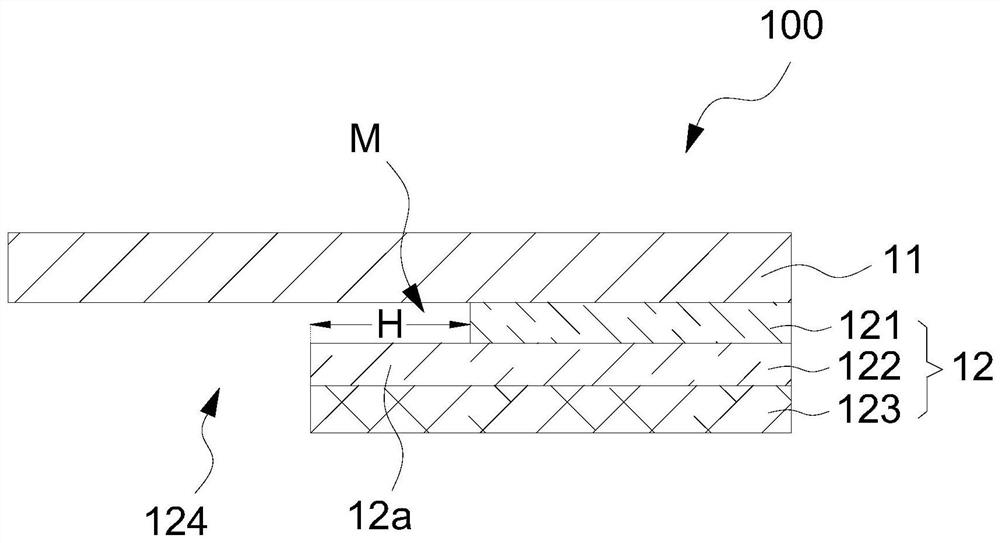
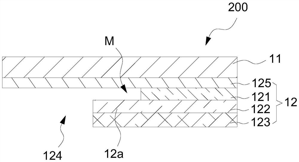
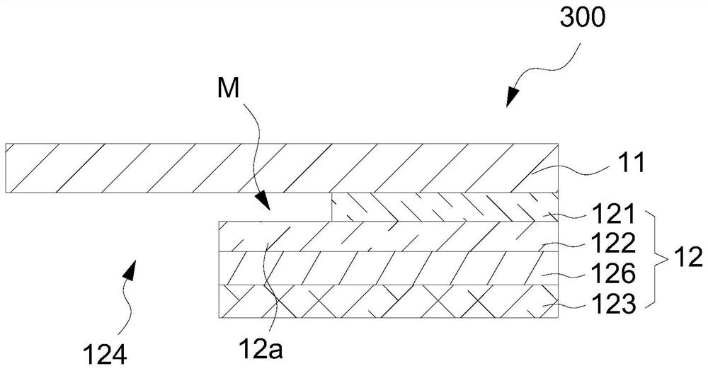
[0057] Please refer to Figure 4 , Figure 4 It is a flow chart of the manufacturing method of the display module according to the embodiment of the present application. A method for manufacturing a display module 100 according to an embodiment of the present application includes the following steps:
[0058] Step S1: sequentially forming a first electrode layer and a second electrode layer on the display panel, the potential of the first electrode layer being lower than that of the second electrode layer;
[0059] Step S2: forming a photoresist layer on the second electrode layer, and patterning the photoresist layer to form openings;
[0060] Step S3: Etching the parts of the first electrode layer and the second electrode layer corresponding to the opening, so that the opening penetrates the first electrode layer and the second electrode layer;
[0061] Step S4: using a stripping solution to strip the photoresist layer, the first electrode layer and the second electrode l...
PUM
| Property | Measurement | Unit |
|---|---|---|
| Width | aaaaa | aaaaa |
Abstract
Description
Claims
Application Information
 - R&D Engineer
- R&D Manager
- IP Professional
- Industry Leading Data Capabilities
- Powerful AI technology
- Patent DNA Extraction
Browse by: Latest US Patents, China's latest patents, Technical Efficacy Thesaurus, Application Domain, Technology Topic.
© 2024 PatSnap. All rights reserved.Legal|Privacy policy|Modern Slavery Act Transparency Statement|Sitemap