Chip synchronous testing device and chip synchronous testing method

A technology of synchronous testing and chip testing, which is applied in the directions of measuring devices, electronic circuit testing, measuring electricity, etc., can solve the problem of inability to synchronously test multiple chips, and achieves the solution of inability to synchronously test multiple chips, and realizes the diversity of types and chips. The effect of improving test efficiency

Pending Publication Date: 2020-12-25
BEIJING SMARTCHIP MICROELECTRONICS TECH COMPANY +1
View PDF6 Cites 2 Cited by
  • Summary
  • Abstract
  • Description
  • Claims
  • Application Information

AI Technical Summary

Problems solved by technology

[0003] The purpose of the embodiments of the present invention is to provide a chip synchronization test device to at least solve the above-mentioned problem that multiple chips cannot be tested synchronously

Method used


Image

  • Chip synchronous testing device and chip synchronous testing method
  • Chip synchronous testing device and chip synchronous testing method
  • Chip synchronous testing device and chip synchronous testing method

Examples


Embodiment Construction

[0025] Specific embodiments of the present invention will be described in detail below in conjunction with the accompanying drawings. It should be understood that the specific embodiments described here are only used to illustrate and explain the present invention, and are not intended to limit the present invention.

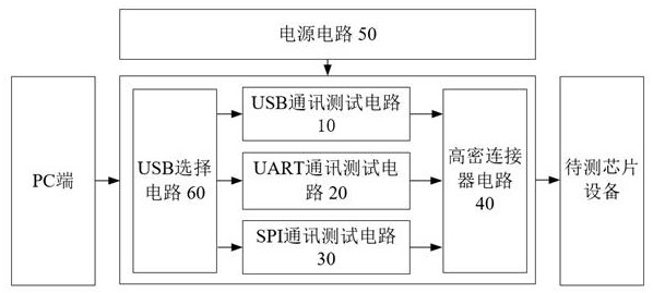
[0026] figure 1 It is a structural diagram of a chip synchronization testing device provided by an embodiment of the present invention. Such as figure 1 As shown, the embodiment of the present invention provides a device capable of realizing multi-chip synchronous testing, the device includes: a communication testing circuit, including a plurality of communication line ports, used for synchronous testing of multiple chips; a high-density connector circuit 40, It is used for the connection between the communication test circuit and the chip device under test. Wherein, described communication test circuit comprises: USB communication test circuit 10, is used fo...


PUM


Abstract

The invention provides a chip synchronous testing device and a chip synchronous testing method, and belongs to the field of chip testing. The chip synchronous testing device comprises communication testing circuits, a high-density connector circuit and a USB selection circuit; the communication testing circuits comprise a plurality of communication line ports and are used for synchronous testing of a plurality of chips; the high-density connector circuit is used for connecting the communication testing circuits and to-be-tested chip equipment; the USB selection circuit is used for switching ona corresponding chip testing interface based on the communication interface type of a to-be-tested chip; the USB selection circuit comprises a 1:3 protocol chip which is used for distinguishing chiptesting paths of different communication interface types. Through the arrangement of chip testing circuits of various interface types, diversity of chip testing types is realized; each type of communication test circuit comprises a plurality of port expansion chips, and a test path is expanded into a plurality of testing paths, so that the synchronous test of t plurality of chips is realized. Theproblem that a plurality of chips cannot be synchronously tested in the prior art is solved.

Description

technical field [0001] The invention relates to the field of chip testing, in particular to a chip synchronous testing device and a chip synchronous testing method. Background technique [0002] At present, the chip industry is developing rapidly, and the chip output is also increasing day by day. In the chip production process, chip testing is a very important step. Most of the existing technologies carry out corresponding test equipment design according to the type of chips produced by themselves. On the one hand, the chips of various manufacturers The test results are uneven, and on the other hand, it also makes the test equipment unable to be popularized. Existing test equipment is mainly realized by fixtures, which need to be customized according to the test chip, and chip test equipment often can only test chips one by one, and cannot realize simultaneous testing of multiple chips, resulting in the existing chip test efficiency cannot meet the chip production requireme...

Claims


Application Information

Patent Timeline
Patent Type & Authority Applications(China)
IPC IPC(8): G01R31/28
CPCG01R31/2851
Inventor 徐靖林魏斌成嵩杜鹏程窦志军王栋
Owner BEIJING SMARTCHIP MICROELECTRONICS TECH COMPANY
Why Eureka
Try Eureka