A high-threshold power semiconductor device and its manufacturing method

A technology of power semiconductors and manufacturing methods, applied in semiconductor/solid-state device manufacturing, semiconductor devices, electrical components, etc., can solve problems such as large gate capacitance, breakdown voltage that cannot meet actual requirements, and small threshold voltage to increase parasitic Capacitance, reduced effective channel width, and increased threshold

Active Publication Date: 2022-04-05
SOUTHEAST UNIV
View PDF0 Cites 0 Cited by
  • Summary
  • Abstract
  • Description
  • Claims
  • Application Information

AI Technical Summary

Problems solved by technology

[0005] In order to solve the problems faced by traditional fin devices such as small threshold voltage, large gate capacitance, and breakdown voltage that cannot meet actual requirements, the present invention proposes a high-threshold power semiconductor device capable of reducing the effective channel width of the device and its manufacture method

Method used


Image

  • A high-threshold power semiconductor device and its manufacturing method
  • A high-threshold power semiconductor device and its manufacturing method
  • A high-threshold power semiconductor device and its manufacturing method

Examples


Embodiment 1

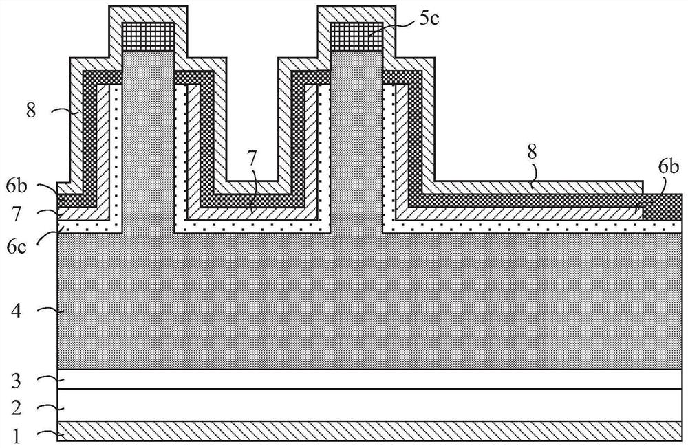
[0055] A high-threshold power semiconductor device according to the present invention includes: a drain metal electrode 1, a substrate 2, a buffer layer 3, and a drift region 4 stacked from bottom to top, and part of the drift region 4 protrudes to form a drift region protrusion A columnar p-region 5a and a columnar n-region 5b are sequentially provided on the drift region protrusion 4a, and a composite column is formed by the drift region protrusion 4a, the columnar p-region 5a and the columnar n-region 5b, and on the drift region 4 The surface, the outside of the composite cylinder and the top of the composite cylinder are provided with a channel layer 6a, the bottom surface of the channel layer 6a is provided with a passivation layer 6b, part of the drift region 4 and part of the channel layer 6a on it, passivation The layer 6b and the composite pillar are divided into the cell area 9, and another part of the drift region 4 and part of the channel layer 6a, the passivation l...

Embodiment 2

[0093] refer to Figure 14 As shown, compared with Embodiment 1, the difference of this embodiment is that the columnar p-region 5a, columnar n-region 5b, channel layer 6a, and heavily doped semiconductor layer 5c of the high-threshold power semiconductor device And the passivation layer 6b, the dielectric layer 6c, the gate metal electrode 7, and the source metal electrode 8 are distributed in straight strips without the passivation layer 6b1, and other structures are the same as in the first embodiment. The manufacturing process of inserting fingers in straight stripes is simpler, and the metal interconnection lines are reduced.

Embodiment 3

[0095] refer to Figure 15 As shown, compared with Embodiment 1, the difference of this embodiment is that the channel layer 6a of the high-threshold power semiconductor device is made of graphene material, and other structures are the same as Embodiment 1. Graphene has extremely high strength and flexibility, which improves the stability of the device; its thermal conductivity is higher than that of gallium nitride materials, so it has higher temperature stability; graphene is the best conductive material at room temperature, and its electronic The mobility is about 140 times that of electrons in silicon, lower than that of copper or silver, and the conductivity can reach 10 6 S / m, so it has lower on-resistance under the same conditions.


PUM

PropertyMeasurementUnit
electrical conductivityaaaaaaaaaa

Abstract

The invention discloses a high-threshold power semiconductor device and a manufacturing method thereof, which include sequentially from bottom to top: a drain metal electrode, a substrate, a buffer layer, and a drift region; A composite column composed of a columnar p-region and a columnar n-region, a channel layer, a passivation layer, a dielectric layer, a heavily doped semiconductor layer, a gate metal electrode and a source metal electrode; the composite column is formed by sequentially depositing P-type semiconductor layer and n-type semiconductor layer are deposited and then formed by etching; channel layer and passivation layer are formed by deposition in sequence; thus the above device is divided into cell area and terminal area, dielectric layer, heavily doped The hetero-semiconductor layer, the gate metal electrode and the source metal electrode only exist in the cell area, and the passivation layer in the terminal area extends upward and wraps around the channel layer. The structure can increase the threshold voltage of the device, improve the blocking characteristics of the device, and reduce the gate capacitance.

Description

technical field [0001] The invention relates to the technical field of semiconductor devices, in particular to a high-threshold power semiconductor device and a manufacturing method thereof. Background technique [0002] With the rapid development of semiconductor device materials and processes, power transistors are more and more widely used in various integrated circuits. At present, the mainstream power devices on the market mainly include silicon-laterally diffused metal oxide semiconductor devices, devices made of gallium arsenide, indium phosphide, and silicon carbide materials. Due to the limitations of the physical properties of the material itself, it cannot meet the needs of the application. Therefore, the development of power devices with new materials is imminent. As a representative of the third-generation semiconductor materials, wide-bandgap GaN materials have become a research hotspot due to their excellent electrical and thermal properties. Gallium nitride...

Claims


Application Information

Patent Timeline
Patent Type & Authority Patents(China)
IPC IPC(8): H01L29/812H01L29/06H01L21/338
CPCH01L29/8122H01L29/8126H01L29/0619H01L29/66856H01L29/1606H01L29/7788H01L29/0657H01L29/42356H01L29/7828H01L29/66666H01L29/0696H01L29/2003H01L29/452H01L29/41741H01L29/1095H01L29/778H01L29/7851
Inventor 孙伟锋张弛辛树轩李胜钱乐葛晨刘斯扬时龙兴
Owner SOUTHEAST UNIV
Why Eureka
Try Eureka