Transistor structure with reinforced total dose radiation resistance

A radiation-hardening, anti-total dose technology, applied in semiconductor devices, electrical components, circuits, etc., can solve the problems of increasing the dynamic power consumption of the circuit, large gate area, reducing the circuit performance, etc., to reduce the channel width, Small aspect ratio, the effect of reducing parasitic leakage

Inactive Publication Date: 2013-01-16
BEIJING MXTRONICS CORP +1
View PDF0 Cites 0 Cited by
  • Summary
  • Abstract
  • Description
  • Claims
  • Application Information

AI Technical Summary

Problems solved by technology

image 3 The disadvantage of the structure shown is that the gate area is large, resulting in a large gate capacitance, which will increase the dynamic power consumption of the circuit and reduce the circuit performance. These shortcomings also limit the application of this structure

Method used


Image

  • Transistor structure with reinforced total dose radiation resistance
  • Transistor structure with reinforced total dose radiation resistance
  • Transistor structure with reinforced total dose radiation resistance

Examples


Embodiment Construction

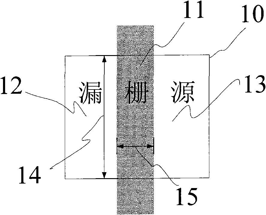
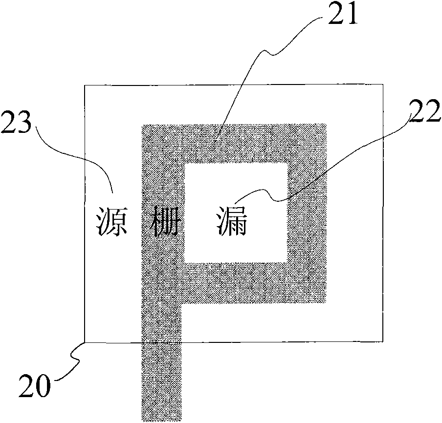
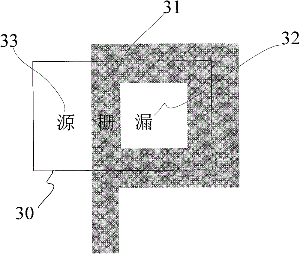
[0020] The anti-total dose radiation-hardened transistor structure of the present invention includes a gate region, a drain region, a source region and a floating region, and the gate region, the drain region, the source region and the floating region are all distributed in the same active region And the gate area separates the active area into a source area, a drain area, and a floating area. There is no intersecting area between the drain area, the source area, and the floating area. The drain area is completely surrounded by the gate area, and the source area is partially surrounded by the gate area. Surrounded or completely surrounded, the floating region is partially surrounded by the gate region; the floating region refers to the region that has the same doping type and the same doping concentration as the source region and the drain region and is not drawn out by wiring. In a transistor, there is one drain region, no less than one source region, and no less than one floa...


PUM


Abstract

The invention discloses a transistor structure with reinforced total dose radiation resistance. An active area is divided by a grid area into a drain area, a source area and a flotation area, the grid area surrounds the drain area completely, a closed parasitic circuit from a source area to a drain area is eliminated, and a total dose radiation resistance reinforcement function is realized. The structure disclosed by the invention solves the problem of parasitic current leakage, which is caused by a total ionizing dose effect, between the source and drain areas, realizes small-size transistorand effectively reduces grid capacitance, thereby better meeting requirements of the high-speed, low-power consumption and reinforced-radiation resistance integrated circuits.

Description

technical field [0001] The invention relates to a transistor structure, in particular to an anti-total dose radiation hardened transistor structure. Background technique [0002] figure 1 Shown is a plan view of a standard conventional metal oxide semiconductor field effect transistor (MOS transistor). The MOS transistor includes a gate region 11 , a drain region 12 and a source region 13 , the gate region 11 divides the active region 10 into a drain region 12 and a source region 13 , and the drain region 12 and the source region 13 have no intersection area. An important parameter determining the characteristics of a transistor is the effective width-to-length ratio of the channel region of the transistor, which is determined by the ratio of the effective channel width 14 to the effective channel length 15 of the transistor. Generally, under other conditions being the same, the larger the effective width-to-length ratio of a transistor, the larger its dynamic power consum...

Claims


Application Information

Patent Timeline
Patent Type & Authority Patents(China)
IPC IPC(8): H01L29/78H01L29/423H01L29/06H01L29/08H01L29/10
Inventor 王亮岳素格
Owner BEIJING MXTRONICS CORP
Why Eureka
Try Eureka