Irradiation protection method for space electronic equipment

An electronic equipment and irradiation technology, which is applied in the field of aerospace, can solve problems such as short-circuit faults of electronic equipment, increase in the weight of aerospace instruments, and potential safety hazards in the combination strength of shielding protection devices and devices, so as to improve the ability to resist total dose and simplify installation Convenience and the effect of reducing the failure rate

Active Publication Date: 2021-10-22
CHANGCHUN INST OF OPTICS FINE MECHANICS & PHYSICS CHINESE ACAD OF SCI
View PDF15 Cites 0 Cited by
  • Summary
  • Abstract
  • Description
  • Claims
  • Application Information

AI Technical Summary

Problems solved by technology

For example, a commonly used method is to thicken the overall shell of the electronic equipment structure so that the equivalent aluminum shielding thickness of the shell meets the radiation resistance design margin. This overall protection scheme will significantly increase the weight of aerospace instruments and does not meet the requirements of aerospace instruments. Lightweight design requirements; Another method is to add shielding measures to sensitive electronic components separately. Since there are many types of device packages, specific shielding protection devices need to be designed for different packages.
It is difficult to install shielding protection devices on some patch packaged devices or TO-3 and TO-39 packaged devices, and the bonding strength between the shielding protection device and the device has potential safety hazards, and it is easy to form detachment and cause short-circuit failure of electronic equipment, which is not conducive to improving space Instrument reliability

Method used


Image

  • Irradiation protection method for space electronic equipment
  • Irradiation protection method for space electronic equipment
  • Irradiation protection method for space electronic equipment

Examples


Embodiment Construction

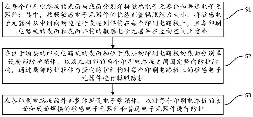
[0030] Hereinafter, embodiments of the present invention will be described with reference to the accompanying drawings. In the following description, the same blocks are denoted by the same reference numerals. With the same reference numerals, their names and functions are also the same. Therefore, its detailed description will not be repeated.

[0031] In order to make the object, technical solution and advantages of the present invention clearer, the present invention will be further described in detail below in conjunction with the accompanying drawings and specific embodiments. It should be understood that the specific embodiments described here are only used to explain the present invention, but not to limit the present invention.

[0032] In the prior art, there are two ways to increase the equivalent aluminum shielding thickness. One is to take all the printed circuit boards as a whole, and set up an electronic box on the outside, and increase the overall thickness of...


PUM


Abstract

The invention provides an irradiation protection method for space electronic equipment. The method comprises the following steps: S1, respectively welding sensitive electronic components on the top surface and the bottom surface of each printed circuit board, wherein the sensitive electronic components are arranged in a concentrated manner, the sensitive electronic components with weak total dose irradiation resistance are placed in the middle, and the sensitive electronic components on the printed circuit boards are overlapped in a vertical space; S2, respectively covering the top surface of the top-layer printed circuit board and the bottom surface of the bottom-layer printed circuit board with local protection box bodies, and fixing a vertical protection structure between two adjacent printed circuit boards so as to carry out irradiation protection on sensitive electronic components on each printed circuit board; and S3, integrally covering each printed circuit board with an electronic box body so as to protect sensitive electronic components and common electronic components on each printed circuit board. On the premise that the weight of the protection device is reduced, the irradiation protection requirement of the electronic equipment can be met, installation is easy, and reliability is high.

Description

technical field [0001] The invention relates to the field of aerospace technology, in particular to a radiation protection method for space electronic equipment. Background technique [0002] Space electronic equipment will be exposed to complex space radiation environments during orbital operation, including space particle radiation environments (such as the Earth’s radiation belts, solar cosmic rays, and galactic cosmic rays, etc.), plasma radiation environments, and ultraviolet radiation environments. The radiation environment will inevitably interact with the satellite to produce various radiation effects, which will cause varying degrees of damage to the functional materials, electronic components and systems on the satellite, and in severe cases, it will cause abnormal work or failure of electronic equipment on orbit. About 40% of all space instrument failures are directly caused by the space environment. Among the instrument failures caused by the space environment, ...

Claims


Application Information

Patent Timeline
Patent Type & Authority Applications(China)
IPC IPC(8): H05K9/00H05K1/14H05K1/18G21F3/00
CPCH05K9/0033H05K9/0037H05K9/0024H05K1/181H05K1/144G21F3/00
Inventor 韩振伟陈波宋克非郭权锋刘世界
Owner CHANGCHUN INST OF OPTICS FINE MECHANICS & PHYSICS CHINESE ACAD OF SCI
Why Eureka
Try Eureka