Gate oxide reinforcement method for improving total dose resistance of MOS (Metal Oxide Semiconductor) device

A MOS device, anti-total dose technology, applied in the fields of semiconductor devices, semiconductor/solid-state device manufacturing, electrical components, etc., can solve the problems of high difficulty and increase the electronic traps of dielectric materials, so as to increase the manufacturing cost and improve the total anti-ionizing dose. Radiation ability, the effect of improving stability

Pending Publication Date: 2022-05-13
58TH RES INST OF CETC
View PDF0 Cites 0 Cited by
  • Summary
  • Abstract
  • Description
  • Claims
  • Application Information

AI Technical Summary

Problems solved by technology

[0006] (1) Modify the medium of the STI isolation area, increase the electron trap of the dielectric material, capture more electrons and neutralize the positive charges brought by the holes, and reduce the positive charge accumulation of the STI isolation area material after ionizing radiation, but involve It is difficult to modify the material and the compatibility between the modified material and the CMOS process;

Method used


Image

  • Gate oxide reinforcement method for improving total dose resistance of MOS (Metal Oxide Semiconductor) device
  • Gate oxide reinforcement method for improving total dose resistance of MOS (Metal Oxide Semiconductor) device
  • Gate oxide reinforcement method for improving total dose resistance of MOS (Metal Oxide Semiconductor) device

Examples


Embodiment Construction

[0042] A gate oxide strengthening method for improving the total dose resistance capability of MOS devices proposed by the present invention will be further described in detail below with reference to the accompanying drawings and specific embodiments. Advantages and features of the present invention will be apparent from the following description and claims. It should be noted that all the drawings are in a very simplified form and use imprecise scales, and are only used to facilitate and clearly assist the purpose of illustrating the embodiments of the present invention.

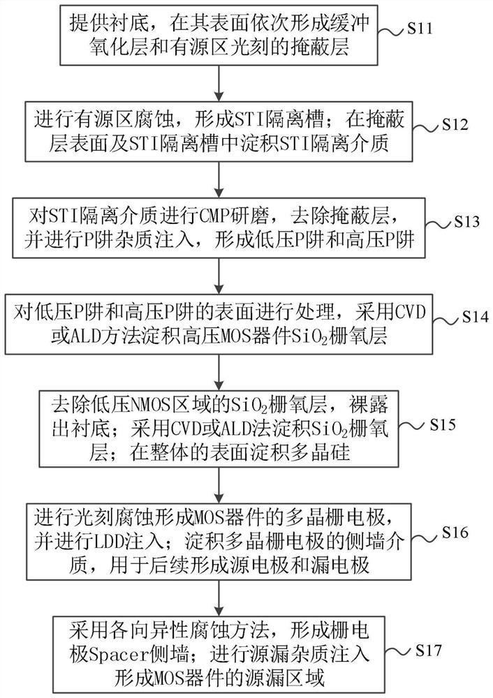
[0043] The invention provides a gate oxide strengthening method for improving the anti-total dose capability of MOS devices, the process of which is as follows figure 1 As shown, the specific process steps are as follows:

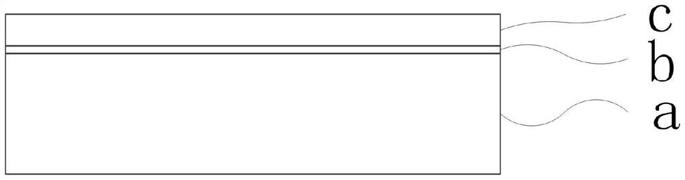
[0044] Step 1: If figure 2 As shown, a bulk silicon, epitaxial material or SOI material substrate a is provided, the thickness of which is the SEMI standard thickness; a buffer oxide...


PUM

PropertyMeasurementUnit
Thicknessaaaaaaaaaa
Thicknessaaaaaaaaaa

Abstract

The invention discloses a gate oxide reinforcement method for improving the total dose resistance of an MOS device, and belongs to the field of microelectronic process manufacturing. According to the invention, a special CVD (chemical vapor deposition) or ALD (atomic layer deposition) method is adopted, and the deposition temperature is less than 800 DEG C, so that the high-quality gate oxide SiO2 medium of the MOS device is prepared; before an MOS device gate oxide layer is deposited through CVD or ALD, SiO2 with the thickness smaller than that of SiO2 is grown on the surface of a silicon substrate through a traditional hot gate oxide process, the interface state density is reduced, and the device parameter stability is improved. According to the manufacturing method, the thermal budget in the manufacturing process of the gate oxide SiO2 of the device can be reduced, the boron doping concentration of P-type Si at the interface of the STI isolation region is improved, the ionization total dose radiation resistance of the device is improved, the number of times of photoetching does not need to be increased, and the manufacturing cost is not increased.

Description

technical field [0001] The invention relates to the technical field of microelectronics manufacturing technology, in particular to a gate oxide reinforcement method for improving the anti-total dose capability of MOS devices. Background technique [0002] MOS devices are the basic components of modern large-scale integrated circuits. They are mainly divided into N-type MOS devices and P-type MOS devices. The conductive carriers of N-type MOS devices are electrons, and the conductive carriers of P-type MOS devices are holes. . In integrated circuits, N-type MOS devices and P-type MOS devices are often combined to design structures of inverters, registers, and SRAM storage units. [0003] When MOS devices work in ionizing radiation environment, SiO in MOS devices 2 The isolation medium will be ionized to form electron-hole pairs, and the electrons will leave the medium area quickly under the action of the electric field, while the holes generated at the same time have a larg...

Claims


Application Information

Patent Timeline
IPC IPC(8): H01L21/285H01L29/423H01L21/336
CPCH01L21/28194H01L21/28211H01L29/66477H01L29/42364
Inventor 王印权郑若成洪根深贺琪胡君彪郝新焱
Owner 58TH RES INST OF CETC
Why Eureka
Try Eureka