Radiation-resistant pip type ono antifuse structure and cmos process integration method

An anti-fuse, anti-radiation technology, applied in the direction of semiconductor/solid-state device components, semiconductor devices, electrical components, etc., can solve the problems affecting the integration of the anti-radiation ONO anti-fuse CMOS process, limiting the integration density of the device process, etc. Achieve the effect of optimizing process integration sequence, enhancing total dose resistance, and improving consistency

Active Publication Date: 2018-10-30
58TH RES INST OF CETC
View PDF6 Cites 0 Cited by
  • Summary
  • Abstract
  • Description
  • Claims
  • Application Information

AI Technical Summary

Problems solved by technology

The traditional structure is made in the N+ active area on the P-type silicon substrate (such as patents: US. Including the antifuse dielectric layer and the antifuse lower plate withstand voltage, the size of the field area limits the integration density of the device process, especially the thermal field of the ONO antifuse CMOS process with a size above 0.8μm to the integrated circuit area It is only suitable for small-scale FPGA and PROM circuit process integration; at the same time, in terms of radiation resistance, it is also necessary to consider the leakage between the field area and the field edge due to the total dose ionization effect. Conventional methods The method of P+ injection cut-off in the active area is adopted, but it is affected by the withstand voltage of the lower plate, which limits the reduction of the area of ​​the ONO anti-fuse unit, which in turn affects the integration of the radiation-resistant ONO anti-fuse CMOS process.

Method used


Image

  • Radiation-resistant pip type ono antifuse structure and cmos process integration method
  • Radiation-resistant pip type ono antifuse structure and cmos process integration method
  • Radiation-resistant pip type ono antifuse structure and cmos process integration method

Examples


Embodiment Construction

[0044] The embodiments listed in the present invention are only used to help understand the present invention, and should not be interpreted as limiting the protection scope of the present invention. For those of ordinary skill in the art, they can also Improvements and modifications are made to the present invention, and these improvements and modifications also fall within the protection scope of the claims of the present invention.

[0045] The present invention will be further described below in conjunction with specific examples.

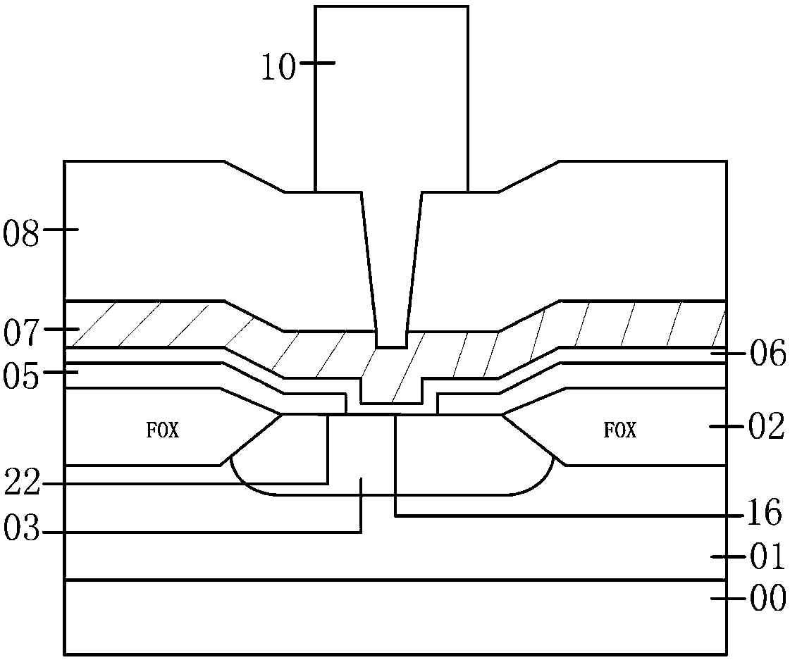
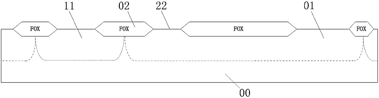
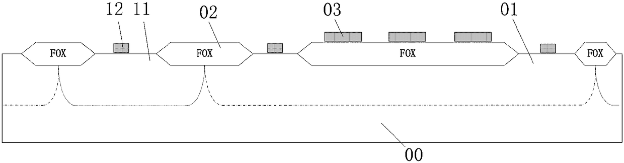
[0046] In order to improve the anti-radiation performance of the unit of the ONO antifuse structure, reduce the area of ​​the integrated unit, optimize the design of the ONO antifuse structure, and improve the integration of the ONO antifuse process, the present invention provides a radiation-resistant PIP type ONO antifuse structure. Such as Figure 11 As shown, the ONO antifuse structure is fabricated on the film layer of the field region 0...


PUM


Abstract

The present invention relates to an anti-radiation PIP-type ONO antifuse structure and a CMOS technology intergrated method. The ONO antifuse structure is made on a field region and comprises an antifuse down plate, an antifuse pitting corrosion masking layer, an ONO antifuse dielectric layer and an antifuse up plate; the antifuse down plate is an N-type saturation doped amorphous silicon film covered on the field region, the side wall of the antifuse down plate employs SPACER protection; an antifuse hole cutting through the antifuse pitting corrosion masking layer is arranged at the right above the antifuse down plate; the antifuse pitting corrosion masking layer covers an active region and the antifuse down plate; the ONO antifuse dielectric layer covers the antifuse pitting corrosion masking layer and fills the antifuse hole; and the antifuse up plate is an N-type saturation doped amorphous silicon film. The unit radiation resistance of the ONO antifuse structure may be improved, the integration unit area may be shortened, the ONO antifuse structure design may be optimized, and the integration level of the ONO antifuse technology may be improved.

Description

technical field [0001] The invention belongs to the technical field of microelectronic integrated circuits, and relates to a radiation-resistant PIP type ONO antifuse structure and a CMOS process integration method, which can be applied to radiation-resistant FPGA / PROM circuit process integration. Background technique [0002] The medium in the ONO anti-fuse unit is a natural anti-radiation structural unit, which has a high anti-radiation total dose capability (1.5Mrad(Si)), and is non-volatile, high reliability, small in size, fast in speed, Advantages such as low power consumption, when not programmed, the ONO antifuse unit exhibits a high resistance state, which can be as high as 10 10 Ohm; after programming with a suitable voltage between the upper and lower electrodes, the ONO antifuse unit exhibits good ohmic resistance characteristics. At present, ONO antifuse technology has been widely used in the fields of computer, communication, automobile, satellite and aerospac...

Claims


Application Information

Patent Timeline
Patent Type & Authority Patents(China)
IPC IPC(8): H01L23/525
Inventor 刘国柱洪根深赵文斌吴建伟朱少立徐静刘佰清
Owner 58TH RES INST OF CETC
Why Eureka
Try Eureka