
mos field effect transistor against total dose effect

A field effect transistor, anti-total dose technology, applied in semiconductor devices, electrical components, circuits, etc., can solve the problems of MOS device failure, increase of N-silicon oxide and silicon interface states, etc.

Active Publication Date: 2022-03-15
NO 47 INST OF CHINA ELECTRONICS TECH GRP
View PDF4 Cites 0 Cited by
  • Summary
  • Abstract
  • Description
  • Claims
  • Application Information

AI Technical Summary

Problems solved by technology

In addition, the total dose effect will increase the interface state of N-silicon oxide and silicon, causing MOS device failure

Method used


Image

  • mos field effect transistor against total dose effect
  • mos field effect transistor against total dose effect
  • mos field effect transistor against total dose effect

Examples


Embodiment Construction

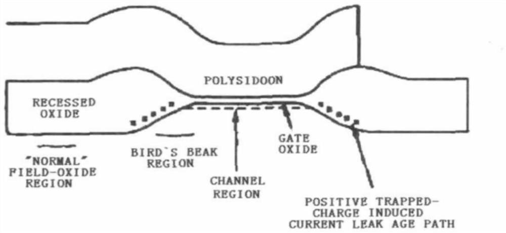
[0035] The source region and the drain region of the common process MOS field effect transistor are implanted into the active region covered by non-polysilicon, such as figure 1The cross-sectional view of a common process MOS field effect transistor is shown. This design creates a parasitic field oxide MOSFET on the silicon gate at the boundary region of the field oxide region and the gate oxide region, because the field oxide layer is very thick, and the charge traps generated by the total dose effect can shift the threshold voltage in the parasitic field oxide MOSFET , In the non-working state, a leakage current is generated in the source region and the drain region of the MOS field effect transistor. Oxide layer leakage current will also be generated in the source region and drain region of the MOS field effect transistor and the N well of the source region and the drain region of the PMOS field effect transistor. Ordinary parasitic field oxide MOSFETs cannot be turned on,...


PUM


Abstract

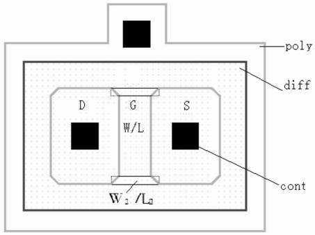
The invention discloses a MOS field effect tube against total dose effect, belonging to the technical field of design of MOS field effect tubes. The field effect transistor uses polysilicon to surround the source and drain regions at the edge of the source region and the drain region. At the same time, the polysilicon covers the edge of the active region to form a butterfly gate structure, because the P tube does not have the problem of edge parasitic transistor inversion. Therefore, only the butterfly grid structure is used for the N tube. The structure is able to reduce the SiO of MOS devices under total dose radiation 2 The radiation-induced trap charges generated in Si / SiO 2 The interface produces a radiation-induced interface state. Therefore, the threshold voltage drift of the MOS device is reduced, the channel carrier mobility is prevented from being reduced, and the leakage current is prevented from increasing. The butterfly gate structure can completely eliminate radiation-induced edge parasitic transistor effects, and is compatible with commercial processes, and integrated circuits designed using this method can have the function of anti-total dose effect as a whole.

Description

technical field [0001] The invention relates to the technical field of design of MOS field effect transistors, in particular to a MOS field effect transistor resistant to total dose effect. Background technique [0002] Satellites, nuclear radiation, and other MOS devices that have been working under low-dose rate high-energy ray radiation conditions for a long time will fail due to radiation-induced device threshold voltage drift, which is the total dose effect. [0003] Since the United States and the Soviet Union conducted nuclear explosion tests over the Pacific Ocean in 1962, causing some satellites to fail, people have gradually paid attention to the behavior of electronic devices in radiation environments and conducted detailed research. In the 1960s, people began to notice that low dose rate radiation for a long time had a great impact on the devices on satellites. By the 1970s, people had a certain initial consensus that the total dose effect can be produced when t...

Claims


Application Information

Patent Timeline
Patent Type & Authority Patents(China)
IPC IPC(8): H01L29/06H01L29/78H01L21/336H01L27/02
CPCH01L27/0207H01L29/0603H01L29/0684H01L29/66477H01L29/78
Inventor 刘淼康晓峰
Owner NO 47 INST OF CHINA ELECTRONICS TECH GRP
Learn More