

Power conversion device
A power conversion device and power line technology, which is applied in the direction of high-efficiency power electronic conversion, output power conversion device, electrical components, etc., can solve problems such as malfunction, and achieve the effect of improving the attenuation effect and suppressing the phenomenon of chain malfunction.
- Summary
- Abstract
- Description
- Claims
- Application Information
AI Technical Summary
Problems solved by technology
Method used
Image

Examples
Embodiment approach 1
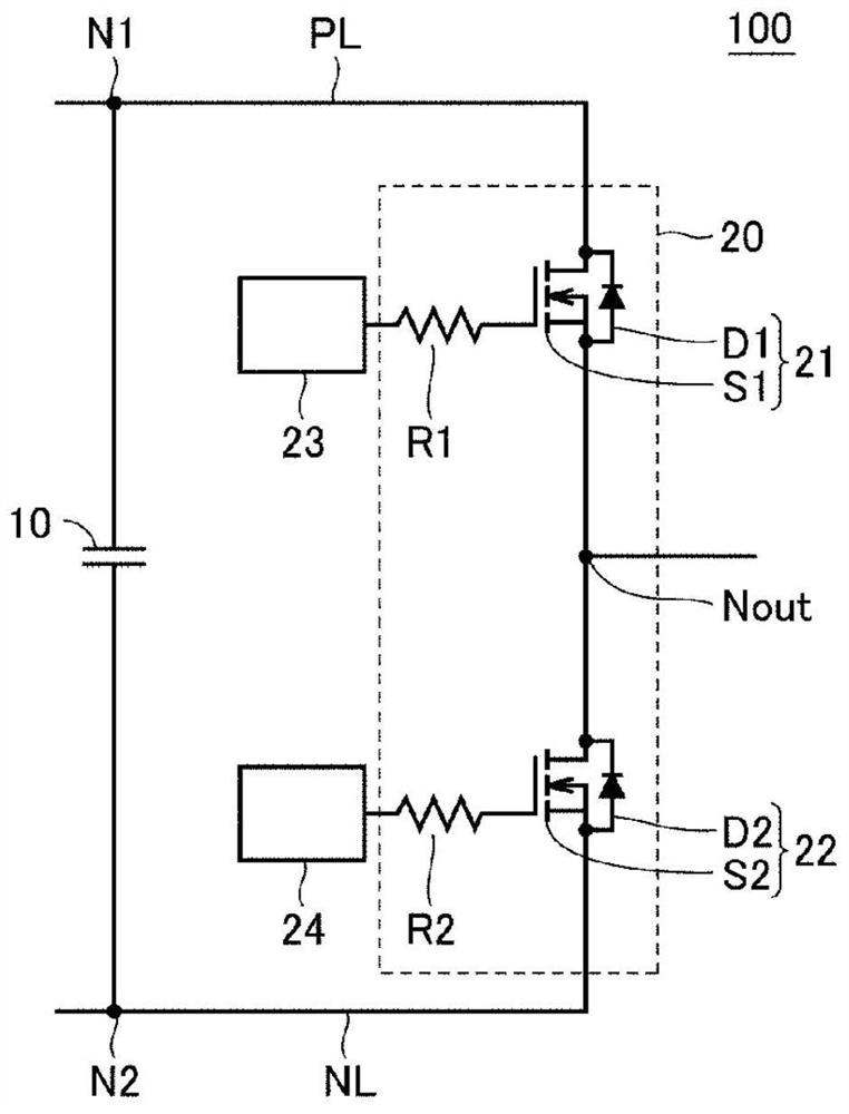
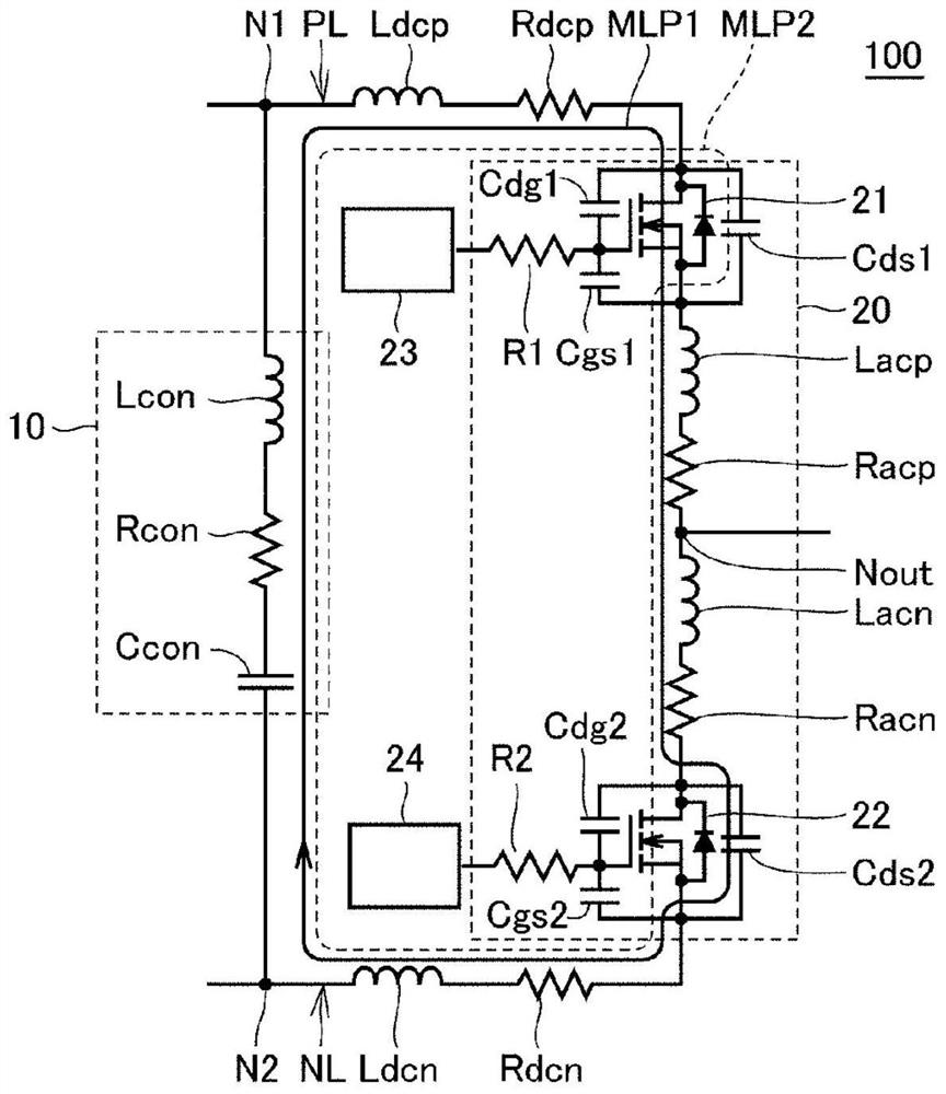
[0035] First, use figure 1 as well as figure 2 , and the basic configuration of the power conversion device to which this embodiment is applied will be described.
[0036] refer to figure 1 The power conversion device 100 includes a high-voltage-side power line PL and a low-voltage-side power line NL, a DC capacitor 10 , a branch circuit 20 , and gate drivers 23 and 24 . The power line PL on the high-voltage side and the power line NL on the low-voltage side are connected to positive and negative sides of a DC power supply (not shown). DC capacitor 10 is connected between node N1 on power line PL and node N2 on power line NL.
[0037] Branch 20 has semiconductor switching elements 21 and 22 connected in series between power lines PL and NL via node Nout. The node Nout corresponds to an "output end" of the branch 20, and is connected to a load via an inductor and / or a capacitor (not shown).
[0038] The semiconductor switching element 21 includes a switch S1 and a diode D...
Embodiment approach 2
[0076] Figure 7 It is a circuit diagram showing a first example of the configuration of the power conversion device according to the second embodiment.
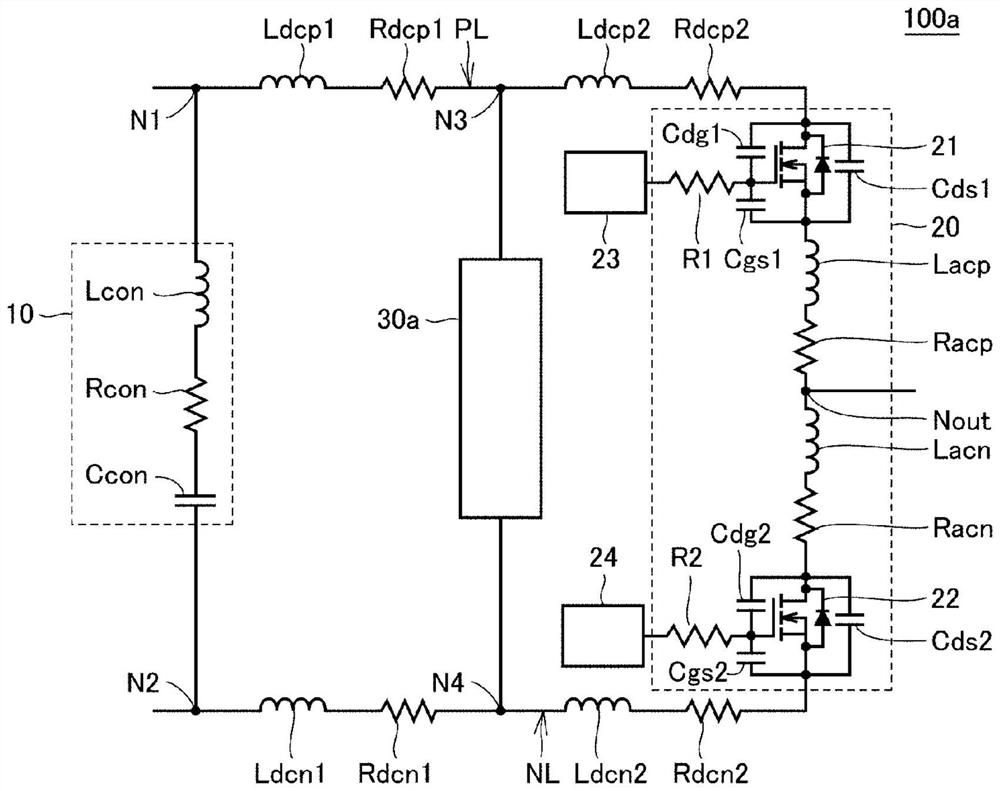
[0077] refer to Figure 7 , the power conversion device 101a of the first example of Embodiment 2 and image 3 as well as Figure 4 The illustrated power conversion device 100 a differs in that it further includes a detection unit 40 and a control unit 50 , and that it does not include an attenuator 30 a but includes an attenuator 31 a.
[0078] Detector 40 is configured to detect voltage and / or current of power lines PL, NL. For example, the voltage of the DC capacitor 10 and / or the current between the DC capacitor 10 and the branch circuit 20 can be detected by the detection unit 40 .
[0079] Attenuator 31a and attenuator 30a ( Figure 4 ) includes an auxiliary switching element 35 connected in series with the resistance element Rsn and the capacitor Csn. The auxiliary switching element 35 includes a switch S3 and a...
Embodiment approach 3
[0116] In Embodiment 3, suppression of a chain malfunction in a power conversion device in which a plurality of branches are connected in parallel will be described.
[0117] Figure 13 It is a circuit diagram showing a basic configuration of a power conversion device to which Embodiment 3 is applied.
[0118] refer to Figure 13 The power conversion device 102 includes a high-voltage-side power line PL and a low-voltage-side power line NL, a DC capacitor 10 , a plurality of branches 20 a and 20 b , and gate drivers 23 and 24 . The power line PL on the high-voltage side and the power line NL on the low-voltage side are connected to positive and negative sides of a DC power supply (not shown).
[0119] Branch 20a has semiconductor switching elements 21a and 22a connected in series between node Nx on power line PL and node Ny on power line NL via node Nouta. The semiconductor switching element 21a includes a switch S1a and a diode D1a connected in antiparallel to the switch S...
PUM
 Abstract
Description
Claims
Application Information