Trench type MOSFET device and preparation method thereof

A trench type, device technology, applied in semiconductor/solid-state device manufacturing, semiconductor devices, electrical components, etc., can solve the problems of difficulty in connecting the bottom p+ region, increase in the size of the original cell, etc., and achieve simple device structure and preparation process, The effect of fine shielding, which is conducive to the promotion of applications

Pending Publication Date: 2021-01-22
安徽芯塔电子科技有限公司
View PDF0 Cites 3 Cited by
  • Summary
  • Abstract
  • Description
  • Claims
  • Application Information

AI Technical Summary

Problems solved by technology

One of the existing technologies is to directly implant ions at the bottom of the trench to form a p+ region shielding structure, but it will bring difficulties in the electrical connection between the bottom p+ region and the sourc

Method used


Image

  • Trench type MOSFET device and preparation method thereof
  • Trench type MOSFET device and preparation method thereof
  • Trench type MOSFET device and preparation method thereof

Examples


Embodiment 1

[0042] The method of the present invention is applicable to various SiC and other semiconductor field effect transistors, such as MOSFETs, IGBTs, etc., and SiC MOSFETs are taken as an example below for illustration.

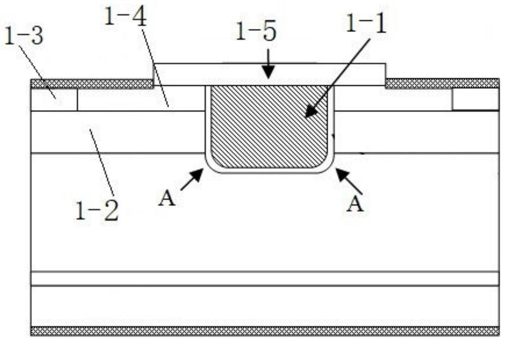
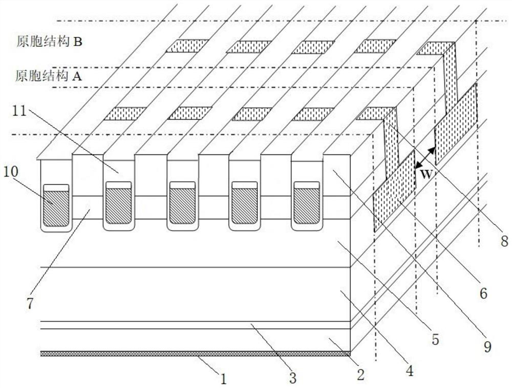
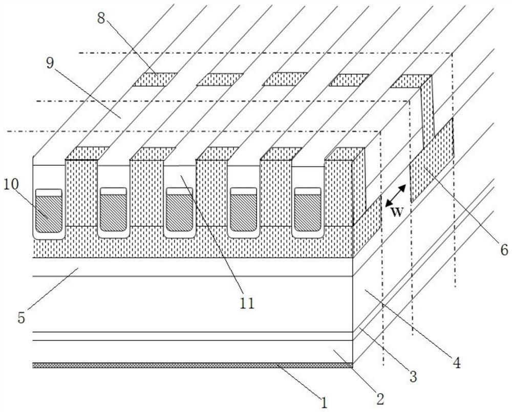
[0043] combine figure 2 with image 3 As shown, this embodiment provides a trench type MOSFET device, which includes drain 1, n+ substrate 2, n+ buffer layer 3, n-drift layer 4, CSL layer 5, p+ buried layer 6, P well 7, p+ region 8 and n+ region 9, gate dielectric, polysilicon gate 10, gate-source isolation dielectric 11, source electrode; the active region of the device is composed of two types of primitive cells with different structures, one type of primitive cells is MOSFET conductive cell A (primary cell cross-section such as figure 2 shown); another type of primitive cell is the primitive cell B that shields the electric field of the trench gate structure (the cross section of the primitive cell is as follows image 3 As shown), the p+ buried layer in ...

Embodiment 2

[0053] The n-type doping and p-type doping mentioned in the embodiment of the present invention are relative terms, and can also be referred to as the first doping and the second doping, that is, the interchange of n-type and p-type is also applicable to devices . Meanwhile, the device structure in the embodiment of the present invention is not only applicable to SiC, but also applicable to other semiconductor materials such as Si, GaN, Ga2O3, etc. In the embodiment of the present invention, SiC is taken as an example.

[0054] Embodiment 2 provides a method for preparing a trench MOSFET device, specifically as follows:

[0055] Such as Figure 4 As shown, an n+ buffer layer 3, an n-drift layer 4, and an n-type CSL layer 5 (current spreading layer) are epitaxially extended on a conductive type n+ substrate 2 in sequence. The concentration and thickness of the n-drift layer 4 are determined by the withstand voltage design of the device, and the general concentration is great...


PUM

PropertyMeasurementUnit
Thicknessaaaaaaaaaa
Thicknessaaaaaaaaaa
Thicknessaaaaaaaaaa

Abstract

The invention relates to the technical field of semiconductors, in particular to a trench type MOSFET device and a preparation method thereof. The trench type MOSFET device sequentially comprises a drain electrode, an n+ substrate, an n+ buffer layer, an n- drift layer, a CSL layer, a p+ buried layer, a p well, a p+ region, an n+ region, a gate medium, a polysilicon gate, a gate source isolation medium and a source electrode from bottom to top. An active region of the device is composed of two types of primitive cells with different structures, one type of primitive cell is an MOSFET conductive primitive cell A, and the other type of primitive cell is a primitive cell B for carrying out electric field shielding on the trench gate structure, and a p+ buried layer in the primitive cell B iselectrically communicated with the source electrode through a p+ region above the p+ buried layer; in the direction parallel to the paper surface, the same type of primitive cells are connected in parallel left and right, and in the depth direction perpendicular to the paper surface, the two types of primitive cells are alternately arranged to form a conductive and shielding area. Through orderedarrangement of the two types of primitive cells by a certain method, the trench gate can be shielded, and very fine primitive cell sizes can be obtained. The device structure and the preparation process are simple, and popularization and application are facilitated.

Description

technical field [0001] The invention relates to the technical field of semiconductors, in particular to a trench type MOSFET device and a preparation method thereof. Background technique [0002] The bandgap width of SiC material is about 3 times that of silicon, and the critical breakdown field strength is about 10 times, so it is very suitable for applications in high-voltage and ultra-high-voltage power fields. SiC trench MOSFETs are the focus of research and product development today. Compared with the low channel mobility of the planar structure SiC MOSFET on the (0001) plane, that is, the silicon plane, the channel of the trench MOSFET is on the crystal plane perpendicular to the (0001) plane, such as on the (11-20) plane, The channel mobility on these planes is higher than that on the (0001) plane. At the same time, the cell size of the trench MOSFET can be smaller than that of the planar MOSFET. Therefore, trench MOSFETs exhibit lower specific on-resistance and hi...

Claims


Application Information

Patent Timeline
IPC IPC(8): H01L29/06H01L29/78H01L21/336
CPCH01L29/0642H01L29/0696H01L29/66068H01L29/7827
Inventor 倪炜江
Owner 安徽芯塔电子科技有限公司
Why Eureka
Try Eureka