micro LED wafer structure and its preparation method

An LED structure and wafer technology, applied in semiconductor devices, electrical components, circuits, etc., can solve problems such as large dislocations in the epitaxial layer of LED chips, improve luminous efficiency, parameter consistency, good contact effect, and reduce the number of strings. light effect

Active Publication Date: 2022-04-26
HCP TECH CO LTD
View PDF4 Cites 0 Cited by
  • Summary
  • Abstract
  • Description
  • Claims
  • Application Information

AI Technical Summary

Problems solved by technology

[0005] In view of the above-mentioned shortcomings of the prior art, the purpose of the present invention is to provide a Micro LED wafer structure and its preparation method, which is used to solve the problem of large dislocations in the epitaxial layer of the LED chip in the prior art.

Method used


Image

  • micro LED wafer structure and its preparation method
  • micro LED wafer structure and its preparation method
  • micro LED wafer structure and its preparation method

Examples


Embodiment 1

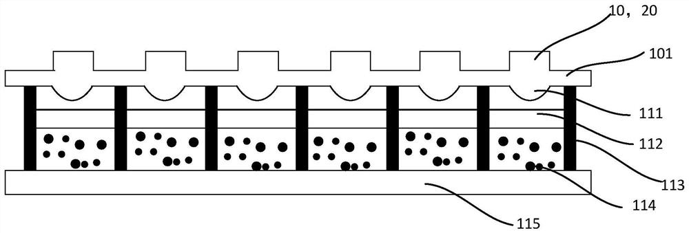
[0051] like Figure 1 to Figure 6 As shown, this embodiment provides a method for preparing a Micro LED wafer structure, and the preparation method includes steps:

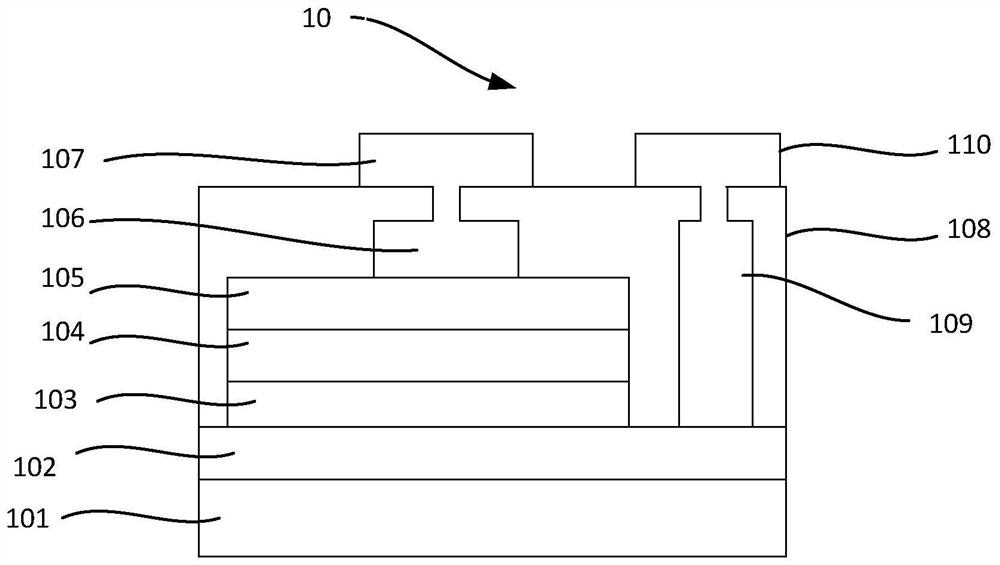
[0052] like figure 1 As shown, step 1) and step 2) are first performed to provide a single crystal substrate 101, 201, the single crystal substrate 101, 201 includes opposite first and second surfaces, on the single crystal substrate An LED structure layer is formed on the first surface of 101, 201, and a plurality of Micro LED arrays are prepared on the single crystal substrate 101, 201 based on the LED structure layer.

[0053] The single crystal substrates 101, 201 may be compound single crystal substrates of Group III and Group V. In this embodiment, the single crystal substrates 101, 201 are selected as GaN single crystal substrates. The present invention uses single crystal substrates 101, 201 (such as single crystal GaN substrates) to grow each layer of the chip, which greatly reduces the dislocation dens...

Embodiment 2

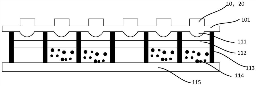
[0076] like Figure 7 ~ Figure 9 As shown, this embodiment also provides a Micro LED wafer structure and its preparation method, the basic steps and basic structure of which are similar to those of Embodiment 1, wherein the difference from Embodiment 1 is that the Micro LED array does not The second conductive layer 109 needs to be prepared in the Micro LED chip. The N electrode 116 (common cathode electrode) of the Micro LED array is formed at the common cathode path and between the Micro LED chips. On the one hand, the common cathode electrode is connected to the driver The circuit connection, on the other hand, reduces the voltage drop generated by the common cathode path, so that the voltage of each Micro LED chip is consistent when it is working. Based on this, the area of ​​the Micro LED chip can be greatly saved, thereby greatly improving the luminescence per unit area of ​​the Micro LED chip. strength.

[0077] As an example, the common cathode electrode may be in the...


PUM


Abstract

The present invention provides a Micro LED wafer structure and a preparation method thereof. The preparation method includes the steps of: 1) providing a single crystal substrate, the single crystal substrate includes an opposite first surface and a second surface, on the surface of the single crystal substrate Form the LED structure layer on the first surface; 2) Prepare multiple Micro LED arrays on the single crystal substrate based on the LED structure layer; 3) Thin the single crystal substrate from the second surface, and then pass the wet etching process Forming a lens array on the second surface; 4) forming a black matrix on the second surface of the single crystal substrate, forming a quantum dot array in the black matrix, and correspondingly setting the quantum dot array, the lens array and the Micro LED array. The invention uses a single crystal substrate to grow each layer of the chip, which greatly reduces the dislocation density. The invention forms a lens array, which can converge the light emitted by each chip on the wafer, can effectively reduce the light crossing between chips, and makes the contact effect between the emitted light and the quantum dots better.

Description

technical field [0001] The invention belongs to the field of design and manufacture of semiconductor light emitters, in particular to a Micro LED wafer structure and a preparation method thereof. Background technique [0002] With the advancement of display technology, the market is concerned about the shortcomings of liquid crystal displays (LCD, Liquid Crystal Display), low contrast, low color gamut, and low response speed, as well as the burn-in and graininess of organic light-emitting displays (OLED, Organic Light Emitting Display). Dissatisfaction with shortcomings such as heavy weight, color cast, and poor light comfort. As a next-generation display technology, Micro LED display technology has the advantages of high contrast, high color gamut, high response speed, ultra-high resolution, and long life. It has both the advantages of LCD and OLED without its disadvantages. Micro LED also has the advantages of flexible display and low energy consumption, and is known as a...

Claims


Application Information

Patent Timeline
Patent Type & Authority Patents(China)
IPC IPC(8): H01L33/00H01L33/38H01L33/58H01L27/15
CPCH01L33/0075H01L33/387H01L33/58H01L27/153H01L2933/0016H01L2933/0058
Inventor 庄文荣孙明卢敬权
Owner HCP TECH CO LTD
Why Eureka
Try Eureka