Circuit board and manufacturing method thereof

A production method and circuit board technology, applied in the directions of printed circuit manufacturing, printed circuits, printed circuit components, etc., can solve the problems of loose adhesion, uneven color and uneven thickness of the cover film, and achieve tight adhesion, The effect of uniform color and lower production cost

Pending Publication Date: 2021-02-02
QING DING PRECISION ELECTRONICS HUAIAN CO LTD +1
View PDF10 Cites 0 Cited by
  • Summary
  • Abstract
  • Description
  • Claims
  • Application Information

AI Technical Summary

Problems solved by technology

On the one hand, the existence of gaps causes problems such as loose adhesion of the cover film, uneven thickness, existence of air bubbles, and uneven color during the surface treatment of the circuit board.

Method used


Image

  • Circuit board and manufacturing method thereof
  • Circuit board and manufacturing method thereof
  • Circuit board and manufacturing method thereof

Examples


Embodiment Construction

[0033] In order to make the technical content disclosed in the present invention more detailed and complete, reference may be made to the drawings and the following various specific embodiments of the present invention, and the same symbols in the drawings represent the same or similar elements. However, those skilled in the art should understand that the examples provided below are not intended to limit the scope of the present invention. In addition, the drawings are for illustrative purposes only and are not drawn to scale according to their actual size.

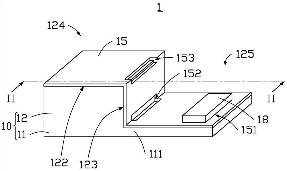
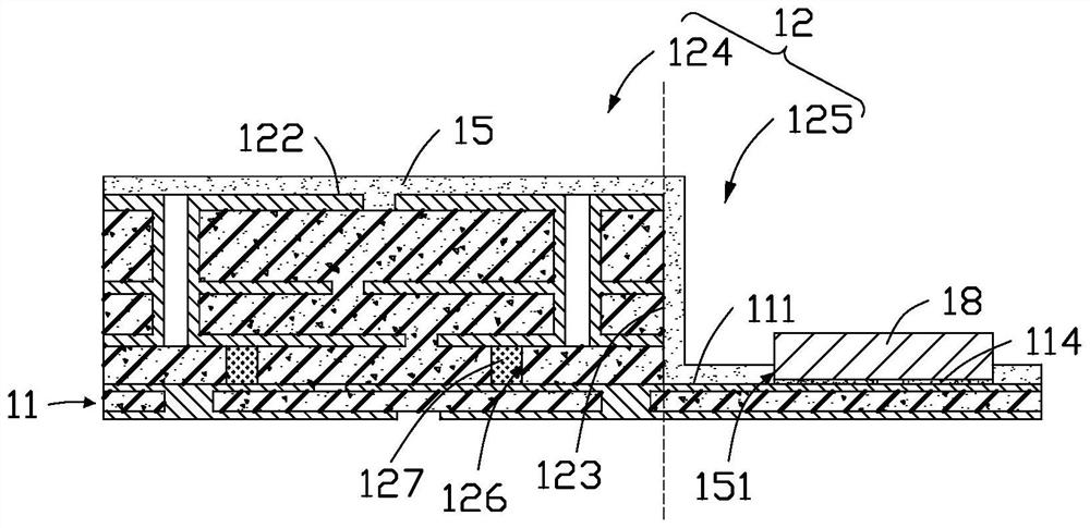
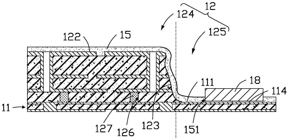
[0034] Such as figure 1 As shown, it is a three-dimensional schematic diagram of a circuit board 1 according to an embodiment of the present invention. Such as figure 2 As shown, it is a schematic cross-sectional view of the circuit board 1 along the direction II-II according to an embodiment of the present invention.

[0035] The circuit board 1 includes a main circuit substrate 10 and a cover film 15, the main circu...


PUM


Abstract

A circuit board comprises a first circuit substrate, wherein the first circuit substrate comprises a first surface, and a contact pad is arranged on the first surface; and a second circuit substrate,wherein the second circuit substrate comprises a second surface and a third side face, the second circuit substrate is arranged on the first surface, the second surface is arranged on the side, away from the first circuit substrate, of the second circuit substrate, the third side face is adjacent to and makes contact with the second surface, and an offset exists between the first surface and the second surface. The circuit board also comprises a cover film, the cover film at least covers the first surface, the second surface and the third side surface, the cover film comprises a first openingand a second opening, the first opening is arranged corresponding to the first surface, at least part of the second opening is arranged corresponding to the third side surface, and the first opening is arranged corresponding to a contact pad so as to expose the contact pad. The invention also provides a manufacturing method of a circuit board.

Description

technical field [0001] The invention relates to a circuit board technology, in particular to a circuit board with high breakage and a manufacturing method of the circuit board. Background technique [0002] With the advancement of technology, circuit boards gradually have more functions. Multifunctional circuit boards are often composite circuit boards. Due to the different structures and wiring requirements of individual electronic components, the surface of composite circuit boards often has unevenness. gap structure. On the one hand, the existence of gaps causes problems such as loose adhesion of the cover film, uneven thickness, existence of air bubbles, and uneven color during the surface treatment of the circuit board. How to solve the above problems needs to be considered by those skilled in the art. Contents of the invention [0003] In view of this, the present invention provides a circuit board and a manufacturing method of the circuit board. [0004] A circui...

Claims


Application Information

Patent Timeline
Patent Type & Authority Applications(China)
IPC IPC(8): H05K1/02H05K3/28
CPCH05K1/02H05K3/281H05K2203/1377
Inventor 徐筱婷何明展沈芾云王之恬
Owner QING DING PRECISION ELECTRONICS HUAIAN CO LTD
Why Eureka
Try Eureka