Display device and preparation method thereof

A technology for display devices and display devices, which is applied in nonlinear optics, instruments, optics, etc., and can solve problems such as information leakage of display screens.

Pending Publication Date: 2021-02-05
GUANGDONG JUHUA PRINTING DISPLAY TECH CO LTD
View PDF8 Cites 0 Cited by
  • Summary
  • Abstract
  • Description
  • Claims
  • Application Information

AI Technical Summary

Problems solved by technology

On the one hand, the wide viewing angle satisfies people's requirements for the viewing effect of video images, and on the other hand, it also leads to the leakage of information carried by the display screen.

Method used


Image

  • Display device and preparation method thereof
  • Display device and preparation method thereof
  • Display device and preparation method thereof

Examples


preparation example Construction

[0081] One embodiment of the present invention provides a method for manufacturing a display device, comprising the following steps:

[0082] Provide the substrate;

[0083] forming a display device on the substrate;

[0084] forming a first alignment layer on a side of the display device away from the substrate;

[0085] forming a liquid crystal layer on the side of the first alignment layer away from the display device;

[0086] Wherein, the initial alignment angle of the liquid crystal layer relative to the display device is 0-30 degrees; or, the initial alignment angle of the liquid crystal layer relative to the display device is 60-90 degrees.

[0087] In one embodiment, further comprising the step of providing a cover plate;

[0088] The steps of forming the liquid crystal layer include:

[0089] Covering the cover plate on the first alignment layer, and forming an accommodation cavity between the cover plate and the first alignment layer;

[0090] A liquid crystal ...

Embodiment 1

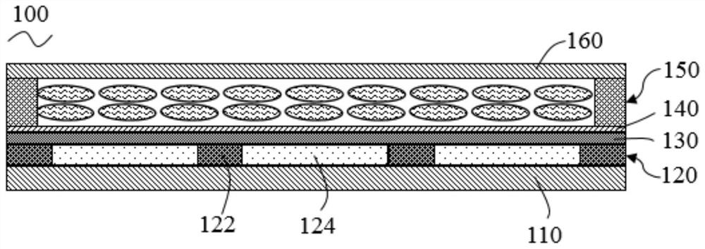
[0095] Example 1 as figure 1 The shown display device 100 and its manufacturing method

[0096] 1) A substrate 110 is provided, and an OLED display device 120 is prepared on the substrate 110 . The display device 120 includes patterned pixel isolation walls 122 and a plurality of light-emitting pixel units 124 separated by the pixel isolation walls 122 .

[0097]2) On the surface of the OLED display device 120, a 30 nm thick gallium oxide thin film is prepared by using a sol-gel (sol-gel method) process as the planar layer 130 . Due to the good light transmittance and strong compactness of the gallium oxide thin film, it can be used not only as a flat layer but also as an encapsulation layer of an OLED display device.

[0098] 3) Coating a layer of polyimide (PI) film with a thickness of 10 nm on the flat layer 130 and preparing an alignment angle of 2° to obtain a first alignment layer 140 with an alignment direction.

[0099] 4) covering the first alignment layer 140 with ...

Embodiment 2

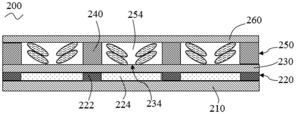
[0101] Example 2 as figure 2 The shown display device 200 and its manufacturing method

[0102] 1) A substrate 210 is provided, and an LCD display device 220 is prepared on the substrate 210 . The display device 220 includes patterned pixel isolation walls 222 and a plurality of light-emitting pixel units 224 separated by the pixel isolation walls 222 .

[0103] 2) On the surface of the LCD display device 220, prepare a layer of 30nm thick PMMA (polymethyl methacrylate) film with a scraping process, then use aluminum as a material, and use an evaporation process to prepare a patterned film on the PMMA film layer. The light-blocking wall 240 , the position of the light-blocking wall 240 corresponds to the position of the pixel isolation wall 222 of the LCD display device 220 , and the height of the light-blocking wall 240 is 50 nm.

[0104] 3) The light-blocking wall 240 divides the surface of the PMMA film into a plurality of regions, wherein each region is divided into a fi...


PUM


Abstract

The invention relates to a display device and a preparation method thereof. The display device comprises a substrate; a display device, wherein the display device is arranged on the substrate; a firstalignment layer which is arranged on one side, far away from the substrate, of the display device; a liquid crystal layerwhich is arranged on one side, far away from the display device, of the firstalignment layer, wherein the initial alignment angle of the liquid crystal layer relative to the display device is 0-30 degrees, or the initial alignment angle of the liquid crystal layer relative tothe display device is 60-90 degrees. According to the display device, the first alignment layer and the liquid crystal layer are arranged on the surface of the display device, liquid crystal moleculesin the liquid crystal layer are directionally arranged in the alignment direction of the first alignment layer through the alignment effect of the first alignment layer, then narrow-view-angle display is achieved, the minimum view angle can reach 90 degrees, and the display effect of the display device cannot be reduced.

Description

technical field [0001] The invention relates to the technical field of light emitting diodes, in particular to a display device and a preparation method thereof. Background technique [0002] In today's society, display devices are ubiquitous and penetrate into every aspect of everyone's life, such as mobile phones, computers, TVs, vehicles, outdoor advertisements, etc. In particular, self-luminous display devices, such as light-emitting diode (LED) display devices, organic light-emitting diode (OLED) display devices, and quantum dot light-emitting diode (QLED) display devices, have the advantages of self-display luminescence, low power consumption, and wide color gamut. , will dominate the display field. With the continuous progress of display technology, the viewing angle of the display device has been widened from the original 120° to more than 170°. However, with the development of technology, the information density carried by the display screen is getting higher and ...

Claims


Application Information

Patent Timeline
IPC IPC(8): G02F1/1337
CPCG02F1/1337
Inventor 李敏敏
Owner GUANGDONG JUHUA PRINTING DISPLAY TECH CO LTD
Why Eureka
Try Eureka