led device and backlight module

An LED device and reflective technology, which is applied to electric solid devices, semiconductor devices, semiconductor devices of light-emitting elements, etc., can solve the problems of the color saturation and light-dark contrast of the display screen, affecting the user's viewing experience, and poor light-emitting performance. Optimize the light output characteristics, improve the viewing experience, and expand the effect of the lighting angle

Active Publication Date: 2022-03-18
FOSHAN NATIONSTAR OPTOELECTRONICS CO LTD
View PDF14 Cites 0 Cited by
  • Summary
  • Abstract
  • Description
  • Claims
  • Application Information

AI Technical Summary

Problems solved by technology

[0004] The main purpose of the present invention is to provide an LED device and a backlight module to solve the problem of poor light output performance caused by the low light extraction efficiency and small light output angle of the LED device in the prior art, and the backlight module manufactured by using the LED device The color saturation and light and dark contrast of the display screen are affected when the group is used on a display device, which affects the user's viewing experience

Method used


Image

  • led device and backlight module
  • led device and backlight module
  • led device and backlight module

Examples


Embodiment 1

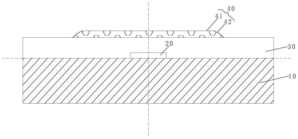
[0028] Such as figure 1 As shown, the LED device includes a substrate 10, a chip 20, a package structure 30 and a top reflective shielding layer 40, wherein the chip 20 is arranged on the substrate 10; the package structure 30 is covered on the substrate 10 and covers the chip 20; the top reflective shielding layer 40 It is arranged on the encapsulation structure 30 and is located at the center of the upper surface of the encapsulation structure 30 and covers a part of the upper surface of the encapsulation structure 30 .

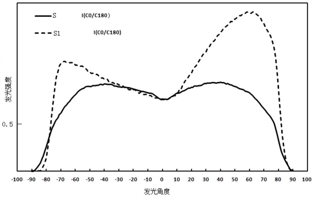
[0029] By arranging the top reflective shielding layer 40 on the package structure 30 and at the center position of the upper surface of the package structure 30, while the top reflective shielding layer 40 covers a part of the upper surface of the package structure 30, so that the light emitted from the front side of the chip 20 Partial reflection is carried out, so that while the LED device has five-sided light emission, the setting of the top reflective ...

Embodiment 2

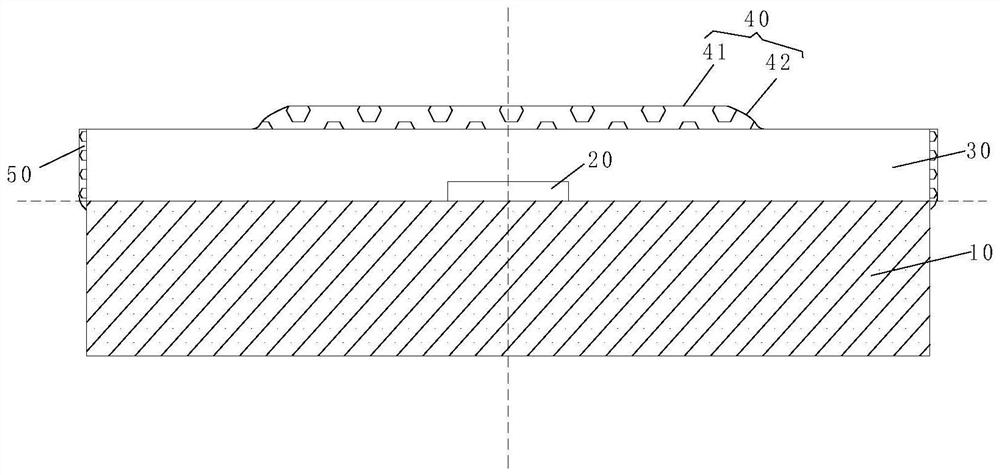
[0038] Such as figure 2 As shown, the difference between this embodiment and Embodiment 1 is that the LED device further includes a peripheral reflective shielding layer 50 , and the peripheral reflective shielding layer 50 covers the outer peripheral side of the encapsulation structure 30 . In this way, by setting the peripheral reflective shielding layer 50 on the outer peripheral side of the packaging structure 30 of the LED device, the circumferential light-emitting characteristics of the LED device are optimized, ensuring that the LED device can emit uniform light in the horizontal direction, and further improving the performance of the LED device. luminescence properties.

[0039] In this embodiment, optionally, the peripheral side of the peripheral reflective shielding layer 50 is a rough surface with an embossed structure.

[0040] Optionally, the embossed structure includes a plurality of prisms or prism grooves distributed in an array. When the embossed structure i...


PUM

PropertyMeasurementUnit
transmittivityaaaaaaaaaa

Abstract

The invention provides an LED device and a backlight module, wherein the LED device includes a substrate, a chip, a package structure and a top reflective shielding layer, wherein the chip is arranged on the substrate; the package structure is set on the substrate and covers the chip; the top reflective The shielding layer is arranged on the packaging structure and is located at the center of the upper surface of the packaging structure and covers a part of the upper surface of the packaging structure. The invention solves the problem of poor light extraction performance caused by the low light output efficiency and small light output angle of LED devices in the prior art, and the color saturation and color saturation of the display screen when the backlight module manufactured by using the LED device is used in a display device. Both light and dark contrast are affected, which affects the user's viewing experience.

Description

technical field [0001] The invention relates to the technical field of LED display lighting, in particular to an LED device and a backlight module. Background technique [0002] With the rapid development of LED technology and the gradual improvement of LED light efficiency, LED devices are widely used in various display devices. [0003] The core light-emitting component of the LED device is the chip. The chip can convert electrical energy into light energy to make the LED device emit light. The chip of the device is packaged, and the existence of the package structure reduces the light output efficiency of the LED device, affects the light output angle, luminous performance and light output uniformity of the LED device, and then uses the color saturation of the display screen of the display device manufactured by the LED device Both light and dark contrast are affected, which affects the viewing experience of the user on the display device. Contents of the invention ...

Claims


Application Information

Patent Timeline
Patent Type & Authority Patents(China)
IPC IPC(8): H01L33/46H01L33/54H01L25/075F21V19/00F21Y115/10
CPCH01L33/46H01L33/54H01L25/0753F21V19/00F21Y2115/10H01L2933/0091H01L33/52H01L33/60
Inventor 李福海董鹏辉陈东子谢志国谢泉
Owner FOSHAN NATIONSTAR OPTOELECTRONICS CO LTD
Why Eureka
Try Eureka