Chip inductor automatic welding device

A technology of automatic welding and chip inductors, which is applied to the assembly of printed circuits, electrical components, and printed circuits with electrical components. It can solve problems such as installation failure, solder waste, and influence on the installation of peripheral components, so as to improve welding efficiency and reduce The effect of saving labor and saving solder paste

Inactive Publication Date: 2021-02-26
广州艺鸣电容器有限公司
View PDF0 Cites 2 Cited by
  • Summary
  • Abstract
  • Description
  • Claims
  • Application Information

AI Technical Summary

Problems solved by technology

[0002] It is often necessary to install SMD inductors on the circuit board. The common installation method of SMD inductors is generally to first apply solder paste on the soldering base and heat it with a hot air gun, and then use tweezers to pick up the SMD inductors and place them on the welding position. After the solder is cooled, the soldering is completed. Due to the small size of the inductor, it is easy to shift the welding position when the tweezers are clamped, resulting in installation failure. In addition, the amount of manual solder paste is not easy to control, which is easy to cause waste of solder. The excess solder will also affect the surrounding area. Installation of components

Method used


Image

  • Chip inductor automatic welding device
  • Chip inductor automatic welding device
  • Chip inductor automatic welding device

Examples


Embodiment Construction

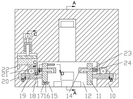
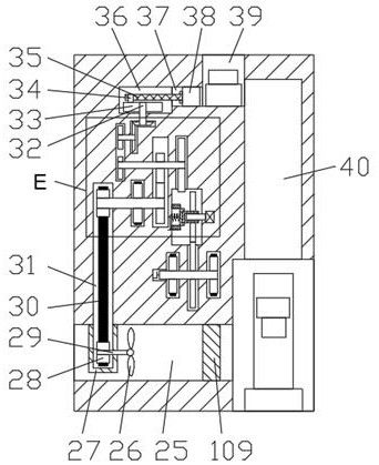
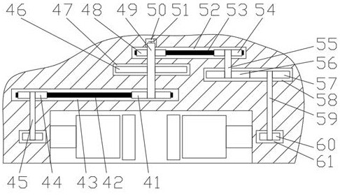
[0020] Combine below Figure 1-6 The present invention is described in detail, wherein, for the convenience of description, the orientations mentioned below are defined as follows:figure 1 The up, down, left, right, front and back directions of the projection relationship itself are the same.

[0021] A chip inductor automatic welding device described in conjunction with accompanying drawings 1-6 includes a main box body 10, and a welding cavity 12 with an opening downward is provided in the main box body 10, and the upper end wall of the welding cavity 12 communicates with A blanking cavity 40 is provided, and the rear end wall of the blanking cavity 40 is connected with an inductor cavity 39 with an upward opening. The rear end wall of the inductor cavity 39 is connected with a push block cavity 37, and the push block cavity 37 The inner sliding fit is connected with a push block 38, the rear end wall of the push block chamber 37 is connected with a runner chamber 36, the re...


PUM


Abstract

The invention relates to the related field of inductors, and discloses a chip inductor automatic welding device which comprises a main box body, a welding cavity with a downward opening is formed in the main box body, a discharging cavity is formed in the upper end wall of the welding cavity in a communicating mode, an inductor cavity with an upward opening is formed in the rear end wall of the discharging cavity in a communicating mode, a push block cavity is formed in the rear end wall of the inductor cavity in a communicating mode, and a push block is connected in the push block cavity in asliding fit way. By automatically smearing and heating soldering paste, then moving a chip inductor to the soldering tin and completing inductor welding after cooling for a certain period of time, automatic welding of the chip inductor is achieved, the workload of operators is reduced, the welding efficiency is improved, meanwhile, the welding position of the inductor can be guaranteed. Moreover,soldering paste can be painted on a welding base in a targeted mode through a welding base distance sensing mechanism, the situation that redundant soldering paste affects installation of other components is effectively prevented, and the soldering paste is saved.

Description

technical field [0001] The invention relates to the related field of inductors, in particular to an automatic welding device for chip inductors. Background technique [0002] It is often necessary to install SMD inductors on the circuit board. The common installation method of SMD inductors is generally to first apply solder paste on the soldering base and heat it with a hot air gun, and then use tweezers to pick up the SMD inductors and place them on the welding position. After the solder is cooled, the soldering is completed. Due to the small size of the inductor, it is easy to shift the welding position when the tweezers are clamped, resulting in installation failure. In addition, the amount of manual solder paste is not easy to control, which is easy to cause waste of solder. The excess solder will also affect the surrounding area. Installation of components. Contents of the invention [0003] The object of the present invention is to provide an automatic welding devi...

Claims


Application Information

Patent Timeline
Patent Type & Authority Applications(China)
IPC IPC(8): H05K3/34
CPCH05K3/341Y02P70/50
Inventor 谭金岜
Owner 广州艺鸣电容器有限公司
Why Eureka
Try Eureka