A kind of polycrystalline silicon ingot and preparation method thereof

A polysilicon ingot and polysilicon technology, applied in the growth of polycrystalline materials, chemical instruments and methods, single crystal growth, etc., can solve the problems of low photoelectric conversion efficiency of batteries, difficulties in industrialization, and many battery stalls, etc., to improve crystal quality and photoelectric conversion efficiency, good crystal quality, and the effect of reducing battery stalls

Active Publication Date: 2022-02-15
JINKO SOLAR CO LTD +1
View PDF0 Cites 0 Cited by
  • Summary
  • Abstract
  • Description
  • Claims
  • Application Information

AI Technical Summary

Problems solved by technology

However, this kind of crystalline silicon cannot solve dislocation problems such as dislocations and subgrain boundaries, especially in the upper and middle parts of the silicon ingot. The rapid proliferation of dislocation defects leads to low and scattered photoelectric conversion efficiency of the battery, many battery stalls, and difficulty in industrialization.

Method used


Image

  • A kind of polycrystalline silicon ingot and preparation method thereof
  • A kind of polycrystalline silicon ingot and preparation method thereof
  • A kind of polycrystalline silicon ingot and preparation method thereof

Examples


preparation example Construction

[0031] The present invention provides a kind of preparation method of polycrystalline silicon ingot, it is characterized in that, comprises the following steps:

[0032] a) Lay the seed crystal on the bottom of the crucible, and then cover the polycrystalline silicon material to obtain the packed silicon material; the seed crystal is single crystal silicon with a single crystal orientation;

[0033] b) Performing directional solidification growth, annealing and cooling sequentially on the loaded silicon material obtained in step a), to obtain polycrystalline silicon ingots.

[0034] In the invention, firstly, the seed crystal is laid on the bottom of the crucible, and then the polysilicon material is covered to obtain the loaded silicon material. In the present invention, there is no special limitation on the source of the crucible, and a commercially available common crucible well known to those skilled in the art can be used. In a preferred embodiment of the present inventi...

Embodiment 1

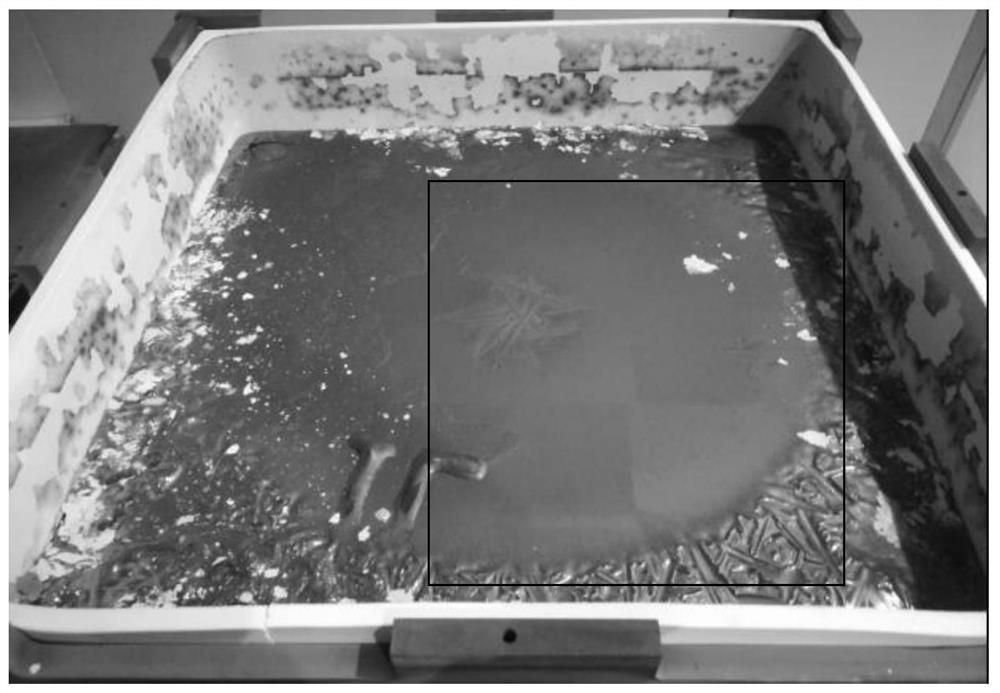
[0063] (1) Seed crystal laying and charging: Arrange the seed crystals on the release layer of the inner bottom of the crucible according to 6mm×6mm, and then put the prepared polysilicon material on the seed crystals to match the size, and put them in at the same time The master alloy is used for doping to obtain the loaded silicon material.

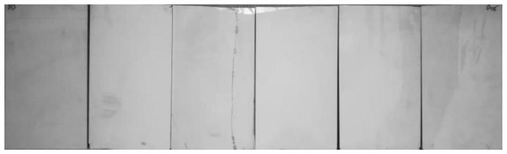
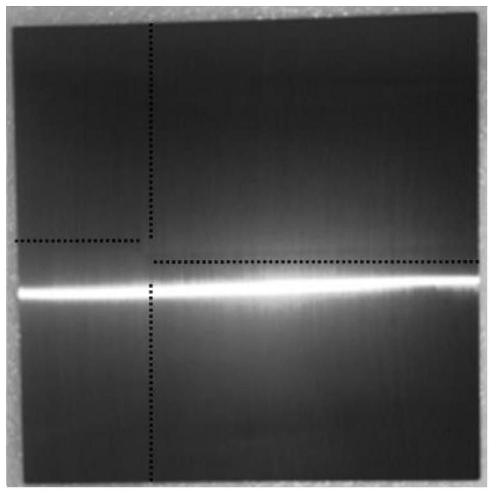
[0064] (2) Directional solidification growth: the crucible filled with silicon material is fitted with guard plates, and placed in a crystal growth furnace for directional solidification growth to obtain grown polysilicon;

[0065] The process of the directional solidification growth is specifically:

[0066] First, place the crucible filled with silicon material in the upper, middle and lower thermal fields and heat it until the temperature of the upper thermal field is 1150°C, the temperature of the middle thermal field is 1100°C, the temperature of the lower thermal field is 1100°C, and the heating time is 280min; then control The t...


PUM

PropertyMeasurementUnit
coating massaaaaaaaaaa

Abstract

The invention provides a method for preparing a polycrystalline silicon ingot, which is characterized in that it comprises the following steps: a) laying a seed crystal on the bottom of a crucible, and then covering the polycrystalline silicon material to obtain a packed silicon material; the seed crystal is a oriented monocrystalline silicon; b) performing directional solidification growth, annealing and cooling in turn on the loaded silicon material obtained in step a) to obtain polycrystalline silicon ingots. Compared with the prior art, the present invention uses monocrystalline silicon with a single crystal orientation as the seed crystal, adopts a specific preparation process to achieve better interaction, and the prepared polycrystalline silicon ingot has a consistent crystal orientation, which can reduce the dislocation density , especially the dislocation density in the upper part of the silicon ingot, thereby improving the crystal quality and photoelectric conversion efficiency. Experimental results show that the polycrystalline silicon ingot prepared by the preparation method provided by the invention has a single crystal orientation consistent with that of the seed crystal; the crystal quality is good, and polycrystalline silicon blocks and polycrystalline silicon wafers can be further obtained; and the photoelectric conversion efficiency can reach more than 19.8%.

Description

technical field [0001] The invention relates to the technical field of polysilicon, and more specifically, relates to a polysilicon ingot and a preparation method thereof. Background technique [0002] In the solar photovoltaic industry, crystalline silicon is the most widely used solar cell material. There are two main types of substrates used in crystalline silicon cells: monocrystalline silicon wafers and polycrystalline silicon wafers. Among them, there is only one crystal grain on the surface of a monocrystalline silicon wafer, and the crystal orientation of the grain is fixed. The single wafer rod is mainly prepared by the pulling method, and then obtained through truncation, squaring, multi-wire cutting and other processes; the surface distribution of polycrystalline silicon wafers has There are multiple crystal grains, and the grains have different sizes, irregular shapes, and inconsistent crystal orientations. They are mainly obtained by preparing polycrystalline s...

Claims


Application Information

Patent Timeline
Patent Type & Authority Patents(China)
IPC IPC(8): C30B28/06C30B29/06
CPCC30B28/06C30B29/06
Inventor 张涛白枭龙欧子杨晏文勇陈骏金浩
Owner JINKO SOLAR CO LTD
Why Eureka
Try Eureka