Microfluidic chip and manufacturing method thereof

A technology of microfluidic chip and manufacturing method, applied in chemical instruments and methods, manufacturing microstructure devices, microstructure technology, etc., can solve problems such as rough edges, blockage of the outlet and inlet of the microfluidic channel of the chip, etc.

Active Publication Date: 2021-02-02
SUZHOU HAN HUA SEMICON CO LTD
View PDF17 Cites 1 Cited by
  • Summary
  • Abstract
  • Description
  • Claims
  • Application Information

AI Technical Summary

Problems solved by technology

[0004] The purpose of the present invention is to provide a microfluidic chip and its manufacturing method to solve the problem that the outlet and inlet of the microfluidic channel of the chip are blocked by impurities when manufacturing the microfluidic chip
In addition, by using single crystal silicon material with the same crystal orientation as the cover sheet and substrate, the problem of rough edges after laser stealth cutting of slivers is solved

Method used


Image

  • Microfluidic chip and manufacturing method thereof
  • Microfluidic chip and manufacturing method thereof
  • Microfluidic chip and manufacturing method thereof

Examples


Embodiment Construction

[0043] The microfluidic chip and its manufacturing method proposed by the present invention will be further described in detail below with reference to the accompanying drawings and specific embodiments. The advantages and features of the present invention will become clearer from the following description. It should be noted that all the drawings are in a very simplified form and use imprecise scales, and are only used to facilitate and clearly assist the purpose of illustrating the embodiments of the present invention. In addition, the structures shown in the drawings are often a part of the actual structure. In particular, each drawing needs to display different emphases, and sometimes uses different scales.

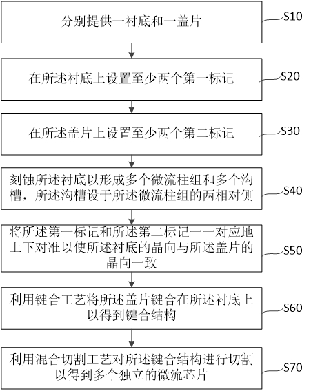
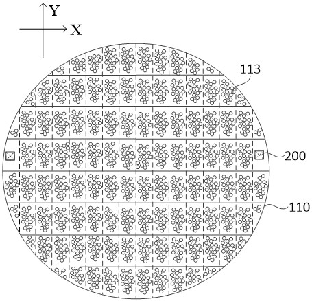
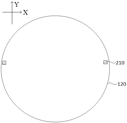
[0044] The invention provides a method for manufacturing a microfluidic chip, referring to figure 1 , figure 1 It is a flow chart of a method for manufacturing a microfluidic chip according to an embodiment of the present invention, and the method for manufacturing...


PUM

PropertyMeasurementUnit
thicknessaaaaaaaaaa

Abstract

The invention provides a manufacturing method of a microfluidic chip. The manufacturing method comprises the following steps of: providing a substrate and a cover plate; setting a first mark on the substrate; setting a second mark on the cover plate; forming a microfluidic column group and a trench on the substrate; aligning the first mark with the second mark; acquiring a bonding structure, wherein the microfluidic column group and the cover plate form a microfluidic channel; and cutting the bonding structure by using a hybrid cutting process to obtain the independent microfluidic chip. Furthermore, the invention also provides the microfluidic chip, which comprises the substrate and the cover plate, wherein the substrate is provided with the microfluidic column group and the trench, and the cover plate is bonded on the substrate. According to the microfluidic chip, the first mark and the second mark are arranged and aligned so that the crystal orientation of the substrate and the crystal orientation of the cover plate can be kept consistent, then the situation that chipping impurities block the microfluidic channel in the chip can be avoided through a mixed cutting process, and the manufacturing yield of the microfluidic chip is increased.

Description

technical field [0001] The invention relates to the technical field of semiconductor device manufacturing, in particular to a microfluidic chip and a manufacturing method thereof. Background technique [0002] Microfluidics (Microfluidics) chip is a micron-level mechanical structure made of semiconductor MEMS technology, which is used to precisely control the movement of micro-scale fluids, thereby controlling the preparation, reaction, detection and other operations of substances in the fluid medium. , chemical, medical and other fields have broad application prospects. Take the atomization microfluidic chip as an example, which is a chip structure with multiple microfluidic channels integrated inside. The microfluidic channels control the compression or intersecting of multiple liquids at the outlet and produce collisions to atomize the liquid into micron-sized Liquid droplets are usually widely used in inhalation drug delivery devices. The atomization microfluidic chip i...

Claims


Application Information

Patent Timeline
Patent Type & Authority Applications(China)
IPC IPC(8): B01L3/00B81C1/00
CPCB01L3/502707B01L2200/10B01L2300/0861B81C1/00119B81C1/00269
Inventor 范谦曹荣兵倪贤锋华斌顾星
Owner SUZHOU HAN HUA SEMICON CO LTD
Why Eureka
Try Eureka